a.
Worst case output voltage for given circuit.
a.
Answer to Problem 14.55P
The worst case output voltage is
Explanation of Solution
Given:
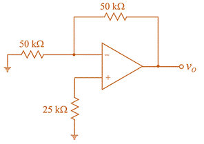
The given circuit is shown below.

Input offset voltage
Average input bias current
Input offset current
Calculation:
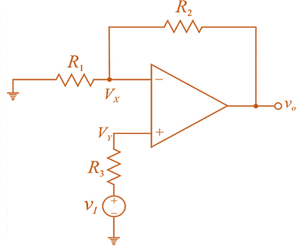
On applying

For given circuit
For an op-amp
Then,
Now, KCL at input nodes:
For op-amp circuit
Now, output voltage due to input bias current and input offset current is,
Due to offset voltage,
From equation (1)
So, the worst case output voltage for the circuit will be,
b.
Worst case output voltage for given circuit.
b.
Answer to Problem 14.55P
The worst case output voltage is
Explanation of Solution
Given:
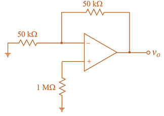
The given circuit is shown below.

Input offset voltage
Average input bias current
Input offset current
Calculation:
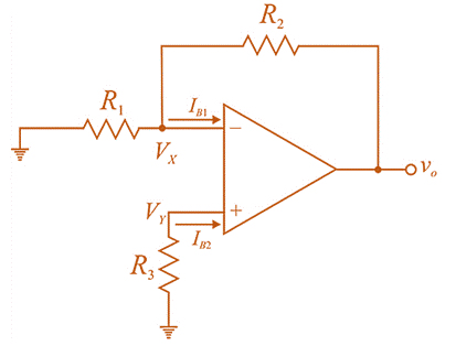
Consider the circuit shwon below.

Apply KCL at non-inverting terminal
For op-amp
So,
Now, KCL at inverting terminal,
Putting
As,
And
Adding (4) and (5)
From (4)
For
For
For the circuit
If offset voltage is negative, then from (1)
Let
Putting
So, the worst case output voltage for circuit is
Want to see more full solutions like this?
Chapter 14 Solutions
MICROELECT. CIRCUIT ANALYSIS&DESIGN (LL)
- the diagram show 4 motor connected to a k-35 controller. I would like detail explanation to know how the circuit work. Is the controller compatible with the motor? The motor shown is series, parallel or both?arrow_forwardplease draw logic diagram pleasearrow_forwardPlease draw the diagrams please thank youarrow_forward
- A plane wave propagating through a medium with &,,-8 μr = 2 has: E = 0.5 e-j0.33z sin (108 t - ẞz) ax V/m. Determine (a) ẞ (b) The loss tangent (c) Wave impedance (d) Wave velocity (e) H fieldarrow_forward2) The phase voltage at the terminals of a balanced three-phase Y-connected load is 2400 V. The load has an impedance of 16+j12 2/6 and is fed from a line having an impedance of 0.10+j0.80 2/6. The Y- connected source at the sending end of the line has a positive phase sequence and an internal impedance of 0.02+j0.16 2/6. Use the a-phase voltage at the load as the reference. a) Construct the a-phase equivalent circuit of the system b) Calculate the line currents IaA, IbB, and Icc c) Calculate the phase voltages at the terminals of the source, Van, Vbn, Vcn- d) Calculate the line voltages at the source, Vab, Vbc and Vca. e) Calculate the internal phase-to-neutral voltages at the source, Va'n, Vb'n, Ve'n,arrow_forward1) • A balanced three-phase circuit has the following characteristics: Y-Y connected The line voltage at the source is Vab = 120√3(0°V • The phase sequence is positive The line impedance is 2+ j3 2/0 The load impedance is 28 + j37 02/0 a) [4 pts] Draw the single phase equivalent circuit for the a-phase. b) [2 pts] Calculate the line current IaA in the a-phase. c) [4 pts] Calculate the line voltage VAB at the load in the a-phase.arrow_forward
- Find the value of V0 using the superposition method. Note: The answer is V0=-428.57mvarrow_forwardDon't use ai to answer I will report you answerarrow_forwardIf a trolley has a 120VDC power supply intended to power auxiliary components such as lights, buzzers, and speakers, how would the speakers connect to that power system? I understand that speakers typically operate on AC, so what is the most efficient way to connect them to the 120VDC setup? Additionally, could you provide an estimate of the power output for the speakers?arrow_forward
- Choose the appropriate answer 1) Maximum dimension of antenna is 0.5m and operating frequency is 9 GHz, thus the radius of reactive near field region is 0.562m 1.265m 2.526m 3.265m 2) If distance between transmitter and receiver is 2km and the signal carrier frequency is 300kHz Rapidly time-varying fields DC field Quasi-static field None 3) The polarization mismatch factor for horizontal polarization wave incident on +z axis is is if the antenna polarization is circular 0.5 зав 0.707 1 4) Ez 0 and Hz #0 (HE modes): This is the case when neither E nor H field is transverse to the direction of wave propagation. They are sometimes referred to as TEM hybrid modes TM TE 5) The normalized radiation intensity of an antenna is represented by: U(6)=cos²(0) cos2 (30), w/s Half-power beamwidth HPBW is...... 28.75 10 0 14.3arrow_forwardChoose the best answer of the following: 1- quasi-static electromagnetic field is the a) low frequency b)high frequency c) time independent d) none of the above 2- Displacement current is taken to be negligible (compared to the conduction current) if a) σ>>wε b)σ << wɛ c) σ =0 d) (a and c) 3- The transmission line act as inductor when it terminated by: a) Open circuit load b) short circuit load c)matched load d)none of the above 4- The scattering aperture equals to the effective aperture when the antenna is: a) Complex conjugate matching b) short circuit c) open circuit d) none of the above 5- The isotropic point source has directivity of: a) Infinity b)1 c) 0 d)1.5arrow_forwardI selected a DC-DC converter capable of delivering 120 VDC from a 600 VDC input. When I reached out to the manufacturer, they asked for the total power consumption the converter would need to handle.To estimate this, I calculated the power requirements for the components that will use the 120 VDC supply: interior lighting, end lights, and buzzers. The breakdown is as follows:- Light Bulbs: 16 bulbs at 10 W each = 160 W- Buzzers: 2 buzzers at 5 W each = 10 W- End Lights: 2 lights at 15 W each = 30 W This results in a total estimated power demand of 200 W.My concern is whether I should request a higher wattage rating for the converter to provide sufficient tolerance and ensure the system operates efficiently without risking an overload. Note: The DC power system is designed specifically for a trolleyarrow_forward
 Electricity for Refrigeration, Heating, and Air C...Mechanical EngineeringISBN:9781337399128Author:Russell E. SmithPublisher:Cengage Learning
