A.
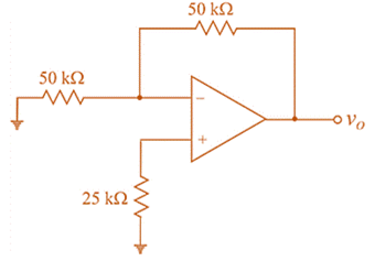
Output voltage due to input bias current and worst case output voltage.
A.
Answer to Problem 14.50P
Output voltage due to input bias current is
Explanation of Solution
Given:
The given circuit is:

Input bias current
Input offset current
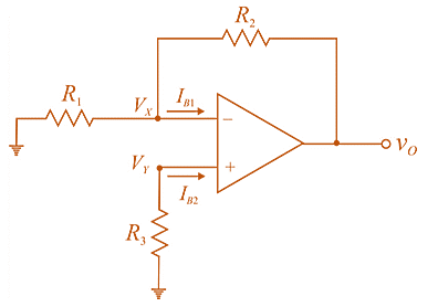
Let the general circuit with input bias currents

Now, using superposition determine
For
The output voltage due to
For
Since,
The output voltage due to
So, the vet output voltage due to both
If
So, the output voltage due to bias current
Now putting the values,
Now, for worst case output
As,
And
Adding (5) and (6)
From (5)
For
For
Assume
For the given circuit
Putting the values in (3)
So, including the effect of input offset current, the worst case output voltage is
B.
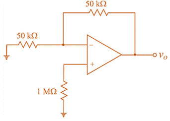
Output voltage due to input bias current and worst case output voltage.
B.
Answer to Problem 14.50P
Output voltage due to input bias current is
Explanation of Solution
Given:
The given circuit is:

Input bias current
Input offset current
Considering equation 4.
Now, for worst case output voltage
Assume
For the given circuit
Putting the values in (3)
So, including the effect of input offset current, the worst case output voltage is
Want to see more full solutions like this?
Chapter 14 Solutions
MICROELECT. CIRCUIT ANALYSIS&DESIGN (LL)
- Choose one of the choices indicated in the parentheses such as the following sentences have correct messing What is the main purpose of a communication system? a) To transmit information from one point to another b) To amplify signals for better reception c) To filter out unwanted noise dy To generate carrier waves for modulation 2. What the purpose of the modulator in a communication system? a) To generate the cares wave for modulation b) To convert the information signal to a modulated signal c) To filter out unwanted noise d) To amplify the modulated signal for transmission Which component in an FM transmitter is responsible for generating the carrier signal? a) Mixer b) Modulator c) Demodulator d) Oscillator 4 For a FM signal v(t) 25 cos (15 deviation 10 (3456 4 24669, 7321 7.21284) 117 10 sm 15501). Maximum frequency 5. In an AM receiver, which component is responsible for separating the modulating signal from the received AM signal? a) Mixer b) Modulator c) Demodulator dy…arrow_forwardQ1. Choose the correct answer: 1. Increasing the amplitude of a square pulse (increases, decreases, maintains not related) the spectrum range in the frequency domain. 2. A continuous FT indicates a signal. (continuous, discrete, periodic non-periodic). the pulse duration is proportional to the amplitude of the signal. (PAM, PWM, PPM, 3. In ASK). . In VSB transmission (both sidebands are used, single sideband is used, single sideband and part of the other sideband, only the vestige of the carrier signal is used). 5. An economic FDM receiver design should contain simultaneous reception, selective reception). 6. In AMI code, the shapes of "1" and "0" are dependent, not related to each other). 7. In FDM the guard band is used to (pilot carrier zero crossing detector, (the same) opposite to each other, next bit increase the overlap between FDM signals, decrease the overlap between FDM signals, increase the baseband bandwidth, decrease the baseband bandwidth). 20 3. Higher number of levels…arrow_forwardIn a railway system with a power source of 600 VDC, I need to achieve a load output of 120 VDC for railway lights. I found a DC-DC converter capable of stepping down 600 VDC to 125 VDC. To obtain 120 VDC from this converter, we can use a voltage divider with the following equation: [R2/(R2+R1)]=120/125=0.96=0.96However, using resistors to achieve the desired output voltage raises some concerns. Is it advisable to use railway-grade resistors for this application? I found some resistors in the range of 1-10k ohms, but I am unsure how they should be connected in the circuit with the lights (the load to be used). I would greatly appreciate any suggestions or schematic diagrams to clarify the best approach for connecting the resistors in this setup.arrow_forward
- Find the valve of the voltage Vx using the THEVENIN equivalent circuit and redo the problem with the NORTON equivalent circuit. Show both the the vinen and Norton circuits. I 12V m 1 ww 3 23 + 43Vx 5 63 миarrow_forwardFind the valve of V using the Thevenin Equivalent Circuit and then determine if the 8 ohm resistor allows maximum power transfer. If not, then what value should the 8 ohm resistor be changed to for maximum power transfer? ZA 6 6 + 22V 83 V 34 2 6 АААА ААААarrow_forwardFind the valve of voltage Vx using the THE VIN IN equivalent circuit ww 8 Show the Theven in Circuit. I 7V ZV m 6 5 M + 4 34 АА 3 1 АААА 9A ↑ 24arrow_forward
 Introductory Circuit Analysis (13th Edition)Electrical EngineeringISBN:9780133923605Author:Robert L. BoylestadPublisher:PEARSON
 Delmar's Standard Textbook Of ElectricityElectrical EngineeringISBN:9781337900348Author:Stephen L. HermanPublisher:Cengage Learning
 Programmable Logic ControllersElectrical EngineeringISBN:9780073373843Author:Frank D. PetruzellaPublisher:McGraw-Hill Education
 Fundamentals of Electric CircuitsElectrical EngineeringISBN:9780078028229Author:Charles K Alexander, Matthew SadikuPublisher:McGraw-Hill Education
 Electric Circuits. (11th Edition)Electrical EngineeringISBN:9780134746968Author:James W. Nilsson, Susan RiedelPublisher:PEARSON
 Engineering ElectromagneticsElectrical EngineeringISBN:9780078028151Author:Hayt, William H. (william Hart), Jr, BUCK, John A.Publisher:Mcgraw-hill Education,


