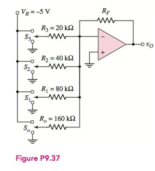
A summing amplifier can be used as a digital-to-analog converter (DAC).An example of a 4-bit DAC is shown in Figure P9.37. When switch S 3 isconnected to the − 5 V supply, the most significant bit is a 3 = 1 ; when S 3 isconnected to ground, the most significant bit is a 3 = 0 . The same conditionapplies to the other switches S 2 , S 1 , and S o , corresponding to bits a 2 , a 1 , and a o , where a o , is the least significant bit. (a) Show that the output voltage isgiven by v o = R F 10 [ a 3 2 + a 2 4 + a 1 8 + a 0 16 ] ( 5 ) where R F is in k Ω . (b) Find the value of R F such that v o = 2.5 V when thedigital input is a 3 a 2 a 1 a 0 = 1000 . (c) Using the results of part (b), find v o for: (i) a 3 a 2 a 1 a 0 = 0001 ,and(ii) a 3 a 2 a 1 a 0 = 1111 .
A summing amplifier can be used as a digital-to-analog converter (DAC).An example of a 4-bit DAC is shown in Figure P9.37. When switch S 3 isconnected to the − 5 V supply, the most significant bit is a 3 = 1 ; when S 3 isconnected to ground, the most significant bit is a 3 = 0 . The same conditionapplies to the other switches S 2 , S 1 , and S o , corresponding to bits a 2 , a 1 , and a o , where a o , is the least significant bit. (a) Show that the output voltage isgiven by v o = R F 10 [ a 3 2 + a 2 4 + a 1 8 + a 0 16 ] ( 5 ) where R F is in k Ω . (b) Find the value of R F such that v o = 2.5 V when thedigital input is a 3 a 2 a 1 a 0 = 1000 . (c) Using the results of part (b), find v o for: (i) a 3 a 2 a 1 a 0 = 0001 ,and(ii) a 3 a 2 a 1 a 0 = 1111 .
Solution Summary: The author explains the expression for the output voltage in Figure 1. Mark the values and redraw the circuit.
A summing amplifier can be used as a digital-to-analog converter (DAC).An example of a 4-bit DAC is shown in Figure P9.37. When switch
S
3
isconnected to the
−
5
V
supply, the most significant bit is
a
3
=
1
; when
S
3
isconnected to ground, the most significant bit is
a
3
=
0
. The same conditionapplies to the other switches
S
2
,
S
1
, and
S
o
, corresponding to bits
a
2
,
a
1
, and
a
o
, where
a
o
, is the least significant bit. (a) Show that the output voltage isgiven by
v
o
=
R
F
10
[
a
3
2
+
a
2
4
+
a
1
8
+
a
0
16
]
(
5
)
where
R
F
is in
k
Ω
. (b) Find the value of
R
F
such that
v
o
=
2.5
V
when thedigital input is
a
3
a
2
a
1
a
0
=
1000
. (c) Using the results of part (b), find
v
o
for: (i)
a
3
a
2
a
1
a
0
=
0001
,and(ii)
a
3
a
2
a
1
a
0
=
1111
.
A dc voltage of unknown value Vand internal resistance Reis connected through a switch
to a lossless transmission line of Zo = 1000. If the first 5 μS of the voltages at z = 0 and z =
L are observed to be as shown below, calculate Vo, RG, the load resistanceR,, and the
transit time T.
100
+ [V]:-0. V
90
[V]:-V
100
75
I, Տ
1,μs
2
4
6
0
2
4
6
A lossless open circuited transmission line behaves as an equivalent capacitance of Ceq =
Tan (BL) Show for BL << 1 that Ceq = C'L where L is the length of the transmission line and
wZo
C' is the lumped parameter capacitance per unit length of the transmission line. Hint: For x
small, Tan(x) = x.
=
A generator with VG 300V and R = 50 is connected to a load R = 750 through a 50 lossless
transmission line of length L = 0.15 m. (a) Compute Zin, the input impedance of the line at the
generator end. (b) Compute and V. (c) Compute the time-average power Pin delivered to the line.
(d) Compute VL, IL, and the time-average power delivered to the load, PL (e) How does Pin compare
to PL? Explain.
Need a deep-dive on the concept behind this application? Look no further. Learn more about this topic, electrical-engineering and related others by exploring similar questions and additional content below.


 Introductory Circuit Analysis (13th Edition)Electrical EngineeringISBN:9780133923605Author:Robert L. BoylestadPublisher:PEARSON
 Delmar's Standard Textbook Of ElectricityElectrical EngineeringISBN:9781337900348Author:Stephen L. HermanPublisher:Cengage Learning
 Programmable Logic ControllersElectrical EngineeringISBN:9780073373843Author:Frank D. PetruzellaPublisher:McGraw-Hill Education
 Fundamentals of Electric CircuitsElectrical EngineeringISBN:9780078028229Author:Charles K Alexander, Matthew SadikuPublisher:McGraw-Hill Education
 Electric Circuits. (11th Edition)Electrical EngineeringISBN:9780134746968Author:James W. Nilsson, Susan RiedelPublisher:PEARSON
 Engineering ElectromagneticsElectrical EngineeringISBN:9780078028151Author:Hayt, William H. (william Hart), Jr, BUCK, John A.Publisher:Mcgraw-hill Education,