Concept explainers
Videos
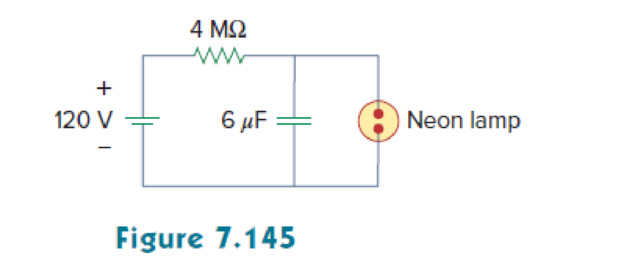
A simple relaxation oscillator circuit is shown in Fig. 7.145. The neon lamp fires when its voltage reaches 75 V and turns off when its voltage drops to 30 V. Its resistance is 120 Ω when on and infinitely high when off.
- (a) For how long is the lamp on each time the capacitor discharges?
- (b) What is the time interval between light flashes?
(a)
Calculate the discharge time of the capacitance when the lamp is on in the given circuit of Figure 7.145.
Answer to Problem 85P
The discharge time of the capacitance is
Explanation of Solution
Given data:
The neon lamp is on when its voltage reaches 75 V and turn off when its voltage drops to 30 V.
The resistance is
Refer to Figure 7.145 in the textbook.
The value of capacitance
Formula used:
Write the general expression to find the complete voltage response for an RC circuit.
Here,
Write the expression to find the time constant for an RC circuit.
Here,
C is the capacitance of the capacitor.
Calculation:
The neon lamp is on when it reaches 75 V. Therefore, the initial capacitor voltage
The neon lamp is off when it drops to 30 V. Therefore, the final capacitor voltage
When the neon lamp on and off, during that time a
Substitute
Substitute the units
Substitute
When the neon lamp is off, the voltage drops to 30 V. That is,
At
Substitute
Taking ln on both sides of the equation.
Rearrange the equation as follows,
Reduce the equation as follows,
Conclusion:
Thus, the discharge time of the capacitance is
(b)
Calculate the time interval between the light flashes.
Answer to Problem 85P
The time interval between the light flashes is
Explanation of Solution
Figure 1 shows the Thevenin resistance at the capacitance terminal.
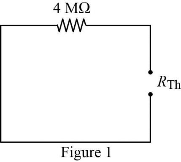
In Figure 1, the Thevenin resistance
Substitute
Substitute the units
At
At
Dividing the equation (6) by (7).
Consider the time interval is,
Substitute
Consider the neon lamp is on when its voltage
Substitute 75 V for
Taking ln on both sides of the equation.
Since, the time interval must be taken as positive value. Therefore,
Conclusion:
Thus, the time interval between the light flashes is
Want to see more full solutions like this?
Chapter 7 Solutions
EBK FUNDAMENTALS OF ELECTRIC CIRCUITS


- 1. The communication channel bandwidth is 25 MHz centered at 1GHz and has a noise power spectral density of 10^-9 W/Hz. The channel loss between the transmitter and receiver is 25dB. The application requires a bit rate of 200Mbps and BER of less than 10^-4. Excluding Mary FSK, Determine the minimum transmit power required.arrow_forward2. An existing system uses noncoherent BASK. The application requires a BER of <10^-5. The current transmit power is 25 Watts. If the system changes to a coherent BPSK modulation scheme, what is the new transmit power required to deliver the same BER?arrow_forward3. You are to design a 9-volt battery operated communication system that must last 3 years without replacing batteries. The communication channel bandwidth is 100 KHz centered at 5.8 GHz. The application requires a BER of <10^-5 and a data rate of 1 Mbps. The channel can be modeled as AWGN with a noise power spectral density of 10^-8 W/Hz. ((a) What modulation scheme would you use? B) what is the required capacity of the batteries? and (c) is the battery commercially available?arrow_forward
- Design a traffic light PIC microcontroller program with Green LED has 3 Sec Yellow LED has 0.5 Sec Red LED has 3 Sec RASAN4SSC20UT 8 RBOINT RB1 9 RB2 U1 PIC16F877A-I/PT 18 19 MCLRVPP RAOANO 20 RA1AN1 30 OSCICLKI 21 RAZAN2VREF-CVREF 31 OSC2CLKO RABAN3VREF+ 22 LED1 LED-3MM 〃 R1 330 RA4TOCKIC1OUT 23 7 VDD 28 VDD 6 VSS 29 VSS 24 LED2 LED-3MM R2 10 330 RB3PGM 11 + 14 RB4 38 RDOPSPO RB5 15 LED3 39 RD1PSP1 40 RD2PSP2 RB6PGC- RB7PGD 17 16 LED-3MM R3 330 41 RD3PSP3 2 RD4PSP4 RCOT1OSOTICKK 3 RDSPSPS RC1T10SICCP24 RD6PSP6 RC2CCP1 5 RD7PSP7 RC3SCKSCL RC4SDISDA 25 REORDANS RCSSDO 27 29 REIWRANG RC6TXCK- RE2CSAN7 RC7RXDT DAWWWW 32 35 36 37 42 43 44 1 12 NO 13 NC 33 NO 34 NCarrow_forward: +0 العنوان I need a detailed drawing with explanation しじ ined sove in peaper Anoting Q4// Draw and Evaluate √√√xy-²sin(y²)dydx PU+96er Lake Ge Q3// Find the volume of the region between the cylinder 2 = y² and the xy- plane that is bounded by the planes x = 1, x = 2, y = -2, and y = 2. T Marrow_forwardFind Va and Vb using Mesh analysisarrow_forward
- Please solve this question step by step and handwritten and do not use chat gpt or ai tools thank you very much!arrow_forwardPlease solve question c and d step by step and handwritten and do not use chat gpt or ai tools thank you very much!arrow_forwardPlease solve questions d,e,f step by step and handwritten and do not use chat gpt or ai tools thank you very much!arrow_forward
 Delmar's Standard Textbook Of ElectricityElectrical EngineeringISBN:9781337900348Author:Stephen L. HermanPublisher:Cengage Learning
 Electricity for Refrigeration, Heating, and Air C...Mechanical EngineeringISBN:9781337399128Author:Russell E. SmithPublisher:Cengage Learning