
Microelectronics: Circuit Analysis and Design
4th Edition
ISBN: 9780073380643
Author: Donald A. Neamen
Publisher: McGraw-Hill Companies, The
expand_more
expand_more
format_list_bulleted
Videos
Textbook Question
Chapter 5, Problem 5.29P
For the circuit shown in Figure P5.29, if
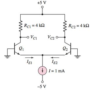
Figure P5.29
Expert Solution & Answer
Want to see the full answer?
Check out a sample textbook solution
Students have asked these similar questions
In the zone refining of silicon, an RF-heater is used to remove trace amounts of impuritiesfrom the silicon. If the silicon has the impurity of 10^14 Co (k = 8*10^-6) what is the purityof the crystal after one pass of the zone refiner? After two passes? Plot concentration as afunction of crystal length from 0 to 8ft (total length of the crystal). The width of the moltenzone is 5”.
Not use ai please
Solve on paper not using AI or chatgpt
Chapter 5 Solutions
Microelectronics: Circuit Analysis and Design
Ch. 5 - An npn transistor is biased in the forwardactive...Ch. 5 - (a) The common-emitter current gains of two...Ch. 5 - An npn transistor is biased in the forwardactive...Ch. 5 - The emitter current in a pnp transistor biased in...Ch. 5 - The output resistance of a bipolar transistor is...Ch. 5 - Assume that IC=1mA at VCE=1V , and that VBE is...Ch. 5 - The openemitter breakdown voltage is BVCBO=200V ,...Ch. 5 - A particular transistor circuit requires a minimum...Ch. 5 - The circuit elements in Figure 5.20(a) are changed...Ch. 5 - The circuit elements in Figure 5.22(a) are V+=3.3V...
Ch. 5 - (a) Verify the results of Example 5.3 with a...Ch. 5 - Consider the pnp circuit in Figure 5.22(a). Assume...Ch. 5 - In the following exercise problems, assume...Ch. 5 - In the following exercise problems, assume...Ch. 5 - The circuit elements in Figure 5.27(a) are changed...Ch. 5 - Using a PSpice simulation, plot the voltage...Ch. 5 - The parameters of the circuit shown in Figure...Ch. 5 - Design the commonbase circuit shown in Figure 5.33...Ch. 5 - The bias voltages in the circuit shown in Figure...Ch. 5 - The bias voltages in the circuit shown in Figure...Ch. 5 - The circuit elements in Figure 5.36(a) are V+=5V ,...Ch. 5 - For the transistor shown in the circuit of Figure...Ch. 5 - For the circuit shown in Figure 5.41, determine...Ch. 5 - Assume =120 for the transistor in Figure 5.42....Ch. 5 - For the transistor in Figure 5.43, assume =90 ....Ch. 5 - (a) Redesign the LED circuit in Figure 5.45(a)...Ch. 5 - The transistor parameters in the circuit in Figure...Ch. 5 - Redesign the inverter amplifier circuit shown in...Ch. 5 - For the circuit shown in Figure 5.44, assume...Ch. 5 - Consider the circuit shown in Figure 5.51(b)....Ch. 5 - [Note: In the following exercises, assume the BE...Ch. 5 - [Note: In the following exercises, assume the B—E...Ch. 5 - Consider the circuit in Figure 5.54(a), let...Ch. 5 - Prob. 5.16EPCh. 5 - The parameters of the circuit shown in Figure...Ch. 5 - Consider the circuit in Figure 5.54(a). The...Ch. 5 - Consider the circuit shown in Figure 5.58. The...Ch. 5 - In the circuit shown in Figure 5.60, the...Ch. 5 - The parameters of the circuit shown in Figure...Ch. 5 - For Figure 5.59, the circuit parameters are...Ch. 5 - In the circuit shown in Figure 5.61, determine new...Ch. 5 - For the circuit shown in Figure 5.63, the circuit...Ch. 5 - (a) Verily the cascode circuit design in Example...Ch. 5 - Prob. 1RQCh. 5 - Prob. 2RQCh. 5 - Prob. 3RQCh. 5 - Define commonbase current gain and commonemitter...Ch. 5 - Discuss the difference between the ac and dc...Ch. 5 - State the relationships between collector,...Ch. 5 - Define Early voltage and collector output...Ch. 5 - Describe a simple commonemitter circuit with an...Ch. 5 - Prob. 9RQCh. 5 - Prob. 10RQCh. 5 - Prob. 11RQCh. 5 - Describe a bipolar transistor NOR logic circuit.Ch. 5 - Describe how a transistor can be used to amplify a...Ch. 5 - Discuss the advantages of using resistor voltage...Ch. 5 - Prob. 15RQCh. 5 - Prob. 16RQCh. 5 - (a) In a bipolar transistor biased in the...Ch. 5 - (a) A bipolar transistor is biased in the...Ch. 5 - (a) The range of ( for a particular type of...Ch. 5 - (a) A bipolar transistor is biased in the...Ch. 5 - Prob. 5.5PCh. 5 - An npn transistor with =80 is connected in a...Ch. 5 - Prob. 5.7PCh. 5 - A pnp transistor with =60 is connected in a...Ch. 5 - (a) The pnp transistor shown in Figure P5.8 has a...Ch. 5 - An npn transistor has a reverse-saturation current...Ch. 5 - Two pnp transistors, fabricated with the same...Ch. 5 - The collector currents in two transistors, A and...Ch. 5 - Prob. 5.13PCh. 5 - Prob. 5.14PCh. 5 - In a particular circuit application, the minimum...Ch. 5 - A particular transistor circuit design requires a...Ch. 5 - For all the transistors in Figure P5.17, =75 . The...Ch. 5 - The emitter resistor values in the circuits show...Ch. 5 - Consider the two circuits in Figure P5.19. The...Ch. 5 - The current gain for each transistor in the...Ch. 5 - Consider the circuits in Figure P5.21. For each...Ch. 5 - (a) The circuit and transistor parameters for the...Ch. 5 - In the circuits shown in Figure P5.23, the values...Ch. 5 - (a) For the circuit in Figure P5.24, determine VB...Ch. 5 - (a) The bias voltages in the circuit shown in...Ch. 5 - The transistor shown in Figure P5.26 has =120 ....Ch. 5 - The transistor in the circuit shown in Figure...Ch. 5 - In the circuit in Figure P5.27, the constant...Ch. 5 - For the circuit shown in Figure P5.29, if =200 for...Ch. 5 - The circuit shown in Figure P5.30 is to be...Ch. 5 - (a) The bias voltage in the circuit in Figure P5.3...Ch. 5 - The current gain of the transistor in the circuit...Ch. 5 - (a) The current gain of the transistor in Figure...Ch. 5 - (a) The transistor shown in Figure P5.34 has =100...Ch. 5 - Assume =120 for the transistor in the circuit...Ch. 5 - For the circuit shown in Figure P5.27, calculate...Ch. 5 - Consider the commonbase circuit shown in Figure...Ch. 5 - (a) For the transistor in Figure P5.38, =80 ....Ch. 5 - Let =25 for the transistor in the circuit shown in...Ch. 5 - (a) The circuit shown in Figure P5.40 is to be...Ch. 5 - The circuit shown in Figure P5.41 is sometimes...Ch. 5 - The transistor in Figure P5.42 has =120 . (a)...Ch. 5 - The commonemitter current gain of the transistor...Ch. 5 - For the circuit shown in Figure P5.44, plot the...Ch. 5 - The transistor in the circuit shown in Figure...Ch. 5 - Consider the circuit in Figure P5.46. For the...Ch. 5 - The current gain for the transistor in the circuit...Ch. 5 - Consider the amplifier circuit shown in Figure...Ch. 5 - For the transistor in the circuit shown in Figure...Ch. 5 - Reconsider Figure P5.49. The transistor current...Ch. 5 - The current gain of the transistor shown in the...Ch. 5 - For the circuit shown in Figure P5.52, let =125 ....Ch. 5 - Consider the circuit shown in Figure P5.53. (a)...Ch. 5 - (a) Redesign the circuit shown in Figure P5.49...Ch. 5 - Prob. 5.55PCh. 5 - Consider the circuit shown in Figure P5.56. (a)...Ch. 5 - (a) Determine the Q-point values for the circuit...Ch. 5 - (a) Determine the Q-point values for the circuit...Ch. 5 - (a) For the circuit shown in Figure P5.59, design...Ch. 5 - Design a bias-stable circuit in the form of Figure...Ch. 5 - Using the circuit in Figure P5.61, design a...Ch. 5 - For the circuit shown in Figure P5.61, the bias...Ch. 5 - (a) A bias-stable circuit with the configuration...Ch. 5 - (a) For the circuit shown in Figure P5.64, assume...Ch. 5 - The dc load line and Q-point of the circuit in...Ch. 5 - The range of ß for the transistor in the circuit...Ch. 5 - The nominal Q-point of the circuit in Figure P5.67...Ch. 5 - (a) For the circuit in Figure P5.67, the value of...Ch. 5 - For the circuit in Figure P5.69, let =100 and...Ch. 5 - Prob. 5.70PCh. 5 - Design the circuit in Figure P5.70 to be bias...Ch. 5 - Consider the circuit shown in Figure P5.72. (a)...Ch. 5 - For the circuit in Figure P5.73, let =100 . (a)...Ch. 5 - Prob. D5.74PCh. 5 - (a) Design a fourresistor bias network with the...Ch. 5 - (a) Design a four-resistor bias network with the...Ch. 5 - (a) A fourresistor bias network is to be designed...Ch. 5 - (a) Design a fourresistor bias network with the...Ch. 5 - For each transistor in the circuit in Figure...Ch. 5 - The parameters for each transistor in the circuit...Ch. 5 - The bias voltage in the circuit shown in Figure...Ch. 5 - Consider the circuit shown in Figure P5.82. The...Ch. 5 - (a) For the transistors in the circuit shown in...Ch. 5 - Using a computer simulation, plot VCE versus V1...Ch. 5 - Using a computer simulation, verify the results of...Ch. 5 - Using a computer simulation, verify the results of...Ch. 5 - Consider a commonemitter circuit with the...Ch. 5 - The emitterfollower circuit shown in Figure P5.89...Ch. 5 - The bias voltages for the circuit in Figure...Ch. 5 - The multitransistor circuit in Figure 5.61 is to...
Knowledge Booster


Learn more about
Need a deep-dive on the concept behind this application? Look no further. Learn more about this topic, electrical-engineering and related others by exploring similar questions and additional content below.Similar questions
- Can you solve for V1 and V2arrow_forwardyou dont need to solve the question i just wanna know the steps and how to find the angle between the voltage difference and the current . thanks so mucharrow_forwardistics of diodes, bipolar junction transistors, and plain the structure, operation, 1. The purpose of doping in semiconductor diodes is: a) To control their electrical properties b) To increase their physical size c) To enhance their mechanical strength d) To improve their thermal stability 2. In electronics production, your team wants to manufacture a very cheap diode rectifier. Which of the following rectifier configurations would you select? a) Half-wave rectifier c) Full-wave rectifier b) Bridge rectifier d) Controlled rectifier 3. The region that a Zener diode operates to provide voltage regulation is: a) Saturation c) Reverse bias b) Breakdown d) Forward bias 4. In NMOS transistors, the depth of the channel is primarily changed by: a) VDS b) lp c) VGS d) None of these 5. NMOS transistors have than PMOS, resulting in better current conduction: b) Long channel a) High mobility c) Low mobility d) Short channel 6. You are working in electronic production, and your team is asked to…arrow_forward
- 8.46 The generator circuit shown in Fig. P8.46 (on page 494) isconnected to a distant load via a long coaxial transmission line.The overall circuit can be modeled as in Fig. P8.46(b), in whichthe transmission line is represented by an equivalent impedanceZline = (5+ j2) W.(a) Determine the power factor of voltage source Vs.(b) Specify the capacitance of a shunt capacitor C that wouldraise the power factor of the source to unity when connectedbetween terminals (a,b). The source frequency is 1.5 kHz.arrow_forward7. MOSFET circuit The MOSFET in the circuit below has V₁ = 1 V and kn = 4 mA/V². a) Is the MOSFET operating in saturation or in the triode region? b) Determine the drain current ID and Vout. + 5 V 5 k Voutarrow_forwardDraw a logic diagram of a 4-bit adder/subtractor then use it to design an Exess-3 to BCD code converter circuit. The circuit has an input (x4 xs x2x) and output (ye ya ya yi)scrarrow_forward
- If waveforms shown in figure below are applied as inputs to a 2-bit comparator (P=P: Po and Q=Q: Q), draw the three output waveforms of the comparator (P>Q, P=Q, Parrow_forwardmicro wavearrow_forwardmicro wavearrow_forwardFor this question, please show how to get the answer using block diagrams. I have included my attempt but I am not close to the answer and I don't understand how to get the T_d(s) expression. Please show the block diagram steps, as in, do not just plug this question into an AI. thank youarrow_forwardOnly expert should attempt this questions, handwritten solution onlyarrow_forwardPlease show formula used and steps as I will study themarrow_forwardarrow_back_iosSEE MORE QUESTIONSarrow_forward_ios
Recommended textbooks for you
 Introductory Circuit Analysis (13th Edition)Electrical EngineeringISBN:9780133923605Author:Robert L. BoylestadPublisher:PEARSON
 Delmar's Standard Textbook Of ElectricityElectrical EngineeringISBN:9781337900348Author:Stephen L. HermanPublisher:Cengage Learning
 Programmable Logic ControllersElectrical EngineeringISBN:9780073373843Author:Frank D. PetruzellaPublisher:McGraw-Hill Education
 Fundamentals of Electric CircuitsElectrical EngineeringISBN:9780078028229Author:Charles K Alexander, Matthew SadikuPublisher:McGraw-Hill Education
 Electric Circuits. (11th Edition)Electrical EngineeringISBN:9780134746968Author:James W. Nilsson, Susan RiedelPublisher:PEARSON
 Engineering ElectromagneticsElectrical EngineeringISBN:9780078028151Author:Hayt, William H. (william Hart), Jr, BUCK, John A.Publisher:Mcgraw-hill Education,
Introductory Circuit Analysis (13th Edition)
Electrical Engineering
ISBN:9780133923605
Author:Robert L. Boylestad
Publisher:PEARSON
Delmar's Standard Textbook Of Electricity
Electrical Engineering
ISBN:9781337900348
Author:Stephen L. Herman
Publisher:Cengage Learning
Programmable Logic Controllers
Electrical Engineering
ISBN:9780073373843
Author:Frank D. Petruzella
Publisher:McGraw-Hill Education
Fundamentals of Electric Circuits
Electrical Engineering
ISBN:9780078028229
Author:Charles K Alexander, Matthew Sadiku
Publisher:McGraw-Hill Education
Electric Circuits. (11th Edition)
Electrical Engineering
ISBN:9780134746968
Author:James W. Nilsson, Susan Riedel
Publisher:PEARSON
Engineering Electromagnetics
Electrical Engineering
ISBN:9780078028151
Author:Hayt, William H. (william Hart), Jr, BUCK, John A.
Publisher:Mcgraw-hill Education,
CMOS Tech: NMOS and PMOS Transistors in CMOS Inverter (3-D View); Author: G Chang;https://www.youtube.com/watch?v=oSrUsM0hoPs;License: Standard Youtube License