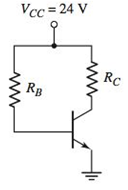
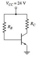
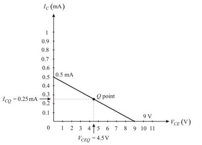
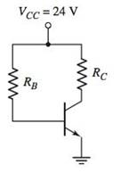
Problem 5.1EP: An npn transistor is biased in the forwardactive mode. The base current is IB=8.50A and the emitter... Problem 5.1TYU: (a) The common-emitter current gains of two transistors are =60 and =150 . Determine the... Problem 5.2TYU: An npn transistor is biased in the forwardactive mode. The base current is IB=5.0A and the collector... Problem 5.3TYU: The emitter current in a pnp transistor biased in the forwardactive mode is IE=1.20mA . The... Problem 5.4TYU: The output resistance of a bipolar transistor is ro=225k at IC=0.8mA . (a) Determine the Early... Problem 5.5TYU: Assume that IC=1mA at VCE=1V , and that VBE is held constant. Determine IC at VCE=10V if: (a) VA=75V... Problem 5.2EP: The openemitter breakdown voltage is BVCBO=200V , the current gain is =120 , and the empirical... Problem 5.6TYU: A particular transistor circuit requires a minimum openbase breakdown voltage of BVCEO=30V . If =100... Problem 5.3EP: The circuit elements in Figure 5.20(a) are changed to VCC=3.3V , VBB=2V , RC=3.2k , and RB=430k .... Problem 5.4EP: The circuit elements in Figure 5.22(a) are V+=3.3V , VBB=1.2V , RB=400k , and RC=5.25k . The... Problem 5.1CAE: (a) Verify the results of Example 5.3 with a PSpice analysis. Use a standard transistor. (b) Repeat... Problem 5.5EP: Consider the pnp circuit in Figure 5.22(a). Assume transistor parameters of VEB(on)=0.7V ,... Problem 5.7TYU: In the following exercise problems, assume VBE(on)=0.7V and VCE(sat)=0.2V . Figure 5.26 Figure for... Problem 5.8TYU: In the following exercise problems, assume VBE(on)=0.7V and VCE(sat)=0.2V . Figure 5.26 Figure for... Problem 5.6EP: The circuit elements in Figure 5.27(a) are changed to RB=200k , RC=4k , and V+=9V . The transistor... Problem 5.2CAE: Using a PSpice simulation, plot the voltage transfer characteristics of the circuit shown in Figure... Problem 5.7EP: The parameters of the circuit shown in Figure 5.30(a) are changed to V+=3.3V , V=3.3V , VBB=0 ,... Problem 5.8EP: Design the commonbase circuit shown in Figure 5.33 such that IEQ=0.125mA and VECQ=2.2V . The... Problem 5.9TYU: The bias voltages in the circuit shown in Figure 5.34 are V+=3.3V and V=3.3V . The measured value of... Problem 5.10TYU: The bias voltages in the circuit shown in Figure 5.35 are V+=5V and V=5V . Assume that =85 .... Problem 5.9EP: The circuit elements in Figure 5.36(a) are V+=5V , VBB=2V , RE=2k , and RB=180k . Assume... Problem 5.10EP: For the transistor shown in the circuit of Figure 540, the common-base current gain is =0.9920 .... Problem 5.11TYU: For the circuit shown in Figure 5.41, determine IE,IB,IC , and VCE , if =75 . (Ans. IB=15.1A ,... Problem 5.12TYU: Assume =120 for the transistor in Figure 5.42. Determine RE such that VCE=2.2V . (Ans. RE=154 )... Problem 5.13TYU: For the transistor in Figure 5.43, assume =90 . (a) Determine VBB such that IE=1.2mA . (b) Find IC... Problem 5.11EP: (a) Redesign the LED circuit in Figure 5.45(a) such that IC1=15mA and IC1/IB1=50 for 1=5V . Use the... Problem 5.12EP: The transistor parameters in the circuit in Figure 5.46(b) are: =40 , VBE(on)=0.7V , and... Problem 5.13EP: Redesign the inverter amplifier circuit shown in Figure 5.48(a) such that the voltage amplification... Problem 5.14TYU: For the circuit shown in Figure 5.44, assume circuit and transistor parameters of RB=240 , VCC=12V ,... Problem 5.14EP: Consider the circuit shown in Figure 5.51(b). Assume VCC=2.8V , =150 , and VBE(on)=0.7V . Design the... Problem 5.15TYU: [Note: In the following exercises, assume the BE cutin voltage is 0.7 V. Also assume the CE... Problem 5.16TYU: [Note: In the following exercises, assume the B—E cutin voltage is 0.7V. Also assume the CE... Problem 5.15EP: Consider the circuit in Figure 5.54(a), let VCC=3.3V , RE=500k , RC=4k , R1=85k , R2=35k , and =150... Problem 5.16EP Problem 5.17TYU: The parameters of the circuit shown in Figure 5.54(a) are VCC=5V , RE=1k , RC=4k , R1=440k and... Problem 5.18TYU: Consider the circuit in Figure 5.54(a). The circuit parameters are VCC=5V and RE=1k . The transistor... Problem 5.17EP: Consider the circuit shown in Figure 5.58. The transistor parameters are =150 and VBE(on)=0.7V . The... Problem 5.18EP: In the circuit shown in Figure 5.60, the parameters are V+=3.3V , V=3.3V , and RB=0 . The transistor... Problem 5.19TYU: The parameters of the circuit shown in Figure 5.57(a) are V+=5V , V=5V , RE=0.5k , and RC=4.5k . The... Problem 5.20TYU: For Figure 5.59, the circuit parameters are IQ=0.25mA , V+=2.5V , V=2.5V , RB=75k , and RC=4k . The... Problem 5.19EP: In the circuit shown in Figure 5.61, determine new values of RC1 and RC2 such that VCEQ1=3.25V and... Problem 5.20EP: For the circuit shown in Figure 5.63, the circuit parameters are V+=12V and RE=2k , and the... Problem 5.4CAE: (a) Verily the cascode circuit design in Example 5.20 using a PSpice simulation. Use standard... Problem 1RQ Problem 2RQ Problem 3RQ Problem 4RQ: Define commonbase current gain and commonemitter current gain. Problem 5RQ: Discuss the difference between the ac and dc commonemitter current gains. Problem 6RQ: State the relationships between collector, emitter, and base currents in a bipolar transistor biased... Problem 7RQ: Define Early voltage and collector output resistance. Problem 8RQ: Describe a simple commonemitter circuit with an npn bipolar transistor and discuss the relation... Problem 9RQ Problem 10RQ Problem 11RQ Problem 12RQ: Describe a bipolar transistor NOR logic circuit. Problem 13RQ: Describe how a transistor can be used to amplify a timevarying voltage. Problem 14RQ: Discuss the advantages of using resistor voltage divider biasing compared to a single base resistor. Problem 15RQ Problem 16RQ Problem 5.1P: (a) In a bipolar transistor biased in the forwardactive region, the base current is iB=2.8A and the... Problem 5.2P: (a) A bipolar transistor is biased in the forwardactive mode. The collector current is iC=726A and... Problem 5.3P: (a) The range of ( for a particular type of transistor is 110180 . Determine the corresponding range... Problem 5.4P: (a) A bipolar transistor is biased in the forwardactive mode. The measured parameters are iE=1.25mA... Problem 5.5P Problem 5.6P: An npn transistor with =80 is connected in a commonbase configuration as shown in Figure P5.6. (a)... Problem 5.7P Problem 5.8P: A pnp transistor with =60 is connected in a commonbase configuration as shown in Figure P5.8. (a)... Problem 5.9P: (a) The pnp transistor shown in Figure P5.8 has a common-base current gain =0.9860 . Determine the... Problem 5.10P: An npn transistor has a reverse-saturation current of IS=51015A and a current gain of =125 . The... Problem 5.11P: Two pnp transistors, fabricated with the same technology, have different junction areas. Both... Problem 5.12P: The collector currents in two transistors, A and B, are both iC=275A . For transistor A, ISA=81016A... Problem 5.13P Problem 5.14P Problem 5.15P: In a particular circuit application, the minimum required breakdown voltages are BVCBO=220V and... Problem 5.16P: A particular transistor circuit design requires a minimum openbase breakdown voltage of BVCEO=50V .... Problem 5.17P: For all the transistors in Figure P5.17, =75 . The results of some measurements are indicated on the... Problem 5.18P: The emitter resistor values in the circuits show in Figures P5.17(a) and (c) may vary by 5 percent... Problem 5.19P: Consider the two circuits in Figure P5.19. The parameters of each transistor are IS=51016A and =90 .... Problem 5.20P: The current gain for each transistor in the circuits shown in Figure P5.20 is =120 . For each... Problem 5.21P: Consider the circuits in Figure P5.21. For each transistor, =120 . Determine IC and VEC for each... Problem 5.22P: (a) The circuit and transistor parameters for the circuit shown in Figure 5.20(a) are VCC=3V ,... Problem 5.23P: In the circuits shown in Figure P5.23, the values of measured parameters are shown. Determine , ,... Problem 5.24P: (a) For the circuit in Figure P5.24, determine VB and IE such that VB=VC . Assume =90 . (b) What... Problem 5.25P: (a) The bias voltages in the circuit shown in Figure P5.25 are changed to V+=3.3V and V=3.3V . The... Problem 5.26P: The transistor shown in Figure P5.26 has =120 . Determine IC and VEC . Plot the load line and the... Problem 5.27P: The transistor in the circuit shown in Figure P5.27 is biased with a constant current in the... Problem 5.28P: In the circuit in Figure P5.27, the constant current is I=0.5mA .If =50 , determine the power... Problem 5.29P: For the circuit shown in Figure P5.29, if =200 for each transistor, determine: (a) IE1 , (b) IE2 ,... Problem 5.30P: The circuit shown in Figure P5.30 is to be designed such that ICQ=0.8mA and VCEQ=2V for the case... Problem D5.31P: (a) The bias voltage in the circuit in Figure P5.3 1 is changed to VCC=9V . The transistor current... Problem 5.32P: The current gain of the transistor in the circuit shown in Figure P5.32 is =150 . Determine IC,IE ,... Problem 5.33P: (a) The current gain of the transistor in Figure P5.33 is =75 . Determine VO for: (i) VBB=0 , (ii)... Problem 5.34P: (a) The transistor shown in Figure P5.34 has =100 . Determine VO for (i) IQ=0.1mA , (ii) IQ=0.5mA ,... Problem 5.35P: Assume =120 for the transistor in the circuit shown in Figure P5.34. Determine IQ such that (a)... Problem 5.36P: For the circuit shown in Figure P5.27, calculate and plot the power dissipated in the transistor for... Problem 5.37P: Consider the commonbase circuit shown in Figure P5.37. Assume the transistor alpha is =0.9920 .... Problem 5.38P: (a) For the transistor in Figure P5.38, =80 . Determine V1 such that VCEQ=6V . (b) Determine the... Problem 5.39P: Let =25 for the transistor in the circuit shown in Figure P5.39. Determine the range of V1 such that... Problem D5.40P: (a) The circuit shown in Figure P5.40 is to be designed such that ICQ=0.5mA and VCEQ=2.5V . Assume... Problem 5.41P: The circuit shown in Figure P5.41 is sometimes used as a thermometer. Assume the transistors Q1 and... Problem 5.42P: The transistor in Figure P5.42 has =120 . (a) Determine VI that produces VO=4V for (i) RE=0k and... Problem 5.43P: The commonemitter current gain of the transistor in Figure P5.43 is =80 . Plot the voltage transfer... Problem 5.44P: For the circuit shown in Figure P5.44, plot the voltage transfer characteristics over the range... Problem 5.45P: The transistor in the circuit shown in Figure P5.45 has a current gain of =40 . Determine RB such... Problem 5.46P: Consider the circuit in Figure P5.46. For the transistor, =50 . Find IB,IC,IE , and VO for (a) VI=0... Problem 5.47P: The current gain for the transistor in the circuit in Figure P5.47 is =60 . Determine RB such that... Problem 5.48P: Consider the amplifier circuit shown in Figure P5.48. Assume a transistor current gain of =120 . The... Problem D5.49P: For the transistor in the circuit shown in Figure P5.49, assume =120 . Design the circuit such that... Problem 5.50P: Reconsider Figure P5.49. The transistor current gain is =150 . The circuit parameters are changed to... Problem 5.51P: The current gain of the transistor shown in the circuit of Figure P5.51 is =100 . Determine VB and... Problem 5.52P: For the circuit shown in Figure P5.52, let =125 . (a) Find ICQ and VCEQ . Sketch the load line and... Problem 5.53P: Consider the circuit shown in Figure P5.53. (a) Determine IBQ,ICQ , and VCEQ for =80 . (b) What is... Problem 5.54P: (a) Redesign the circuit shown in Figure P5.49 using VCC=9V such that the voltage drop across RC is... Problem 5.55P Problem 5.56P: Consider the circuit shown in Figure P5.56. (a) Determine RTH,VTH,IBQ,ICQ , and VECQ for =90 . (b)... Problem 5.57P: (a) Determine the Q-point values for the circuit in Figure P5.57. Assume =50 . (b) Repeat part (a)... Problem 5.58P: (a) Determine the Q-point values for the circuit in Figure P5.58. Assume =50 . (b) Repeat part (a)... Problem D5.59P: (a) For the circuit shown in Figure P5.59, design a biasstable circuit such that ICQ=0.8mA and... Problem D5.60P: Design a bias-stable circuit in the form of Figure P5.59 with =120 such that ICQ=0.8mA , VCEQ=5V ,... Problem D5.61P: Using the circuit in Figure P5.61, design a bias-stable amplifier such that the Q-point is in the... Problem D5.62P: For the circuit shown in Figure P5.61, the bias voltages are changed to V+=3V and V=3V . (a) Design... Problem 5.63P: (a) A bias-stable circuit with the configuration shown in Figure P5.6 1 is to be designed such that... Problem D5.64P: (a) For the circuit shown in Figure P5.64, assume that the transistor current gain is =90 and that... Problem 5.65P: The dc load line and Q-point of the circuit in Figure P5.65(a) are shown in Figure P5.65(b). For the... Problem D5.66P: The range of ß for the transistor in the circuit in Figure P5.66 is 80120 . Design a biasstable... Problem D5.67P: The nominal Q-point of the circuit in Figure P5.67 is ICQ=1mA and VCEQ=5V , for =60 . The current... Problem D5.68P: (a) For the circuit in Figure P5.67, the value of VCC is changed to 3 V. Let RC=5RE and =120 .... Problem D5.69P: For the circuit in Figure P5.69, let =100 and RE=3k . Design a biasstable circuit such that VE=0 .... Problem 5.70P Problem D5.71P: Design the circuit in Figure P5.70 to be bias stable and to provide nominal Q-point values of... Problem D5.72P: Consider the circuit shown in Figure P5.72. (a) The nominal transistor current gain is =80 . Design... Problem 5.73P: For the circuit in Figure P5.73, let =100 . (a) Find VTH and RTH for the base circuit. (b) Determine... Problem D5.74P Problem D5.75P: (a) Design a fourresistor bias network with the configuration shown in Figure P5.6 1 to yield Qpoint... Problem D5.76P: (a) Design a four-resistor bias network with the configuration shown in FigureP5.61 to yield Q-point... Problem D5.77P: (a) A fourresistor bias network is to be designed with the configuration shown in Figure P5.77. The... Problem D5.78P: (a) Design a fourresistor bias network with the configuration shown in Figure P5.77 such that the... Problem 5.79P: For each transistor in the circuit in Figure P5.79, =120 and the BE turn on voltage is 0.7 V.... Problem 5.80P: The parameters for each transistor in the circuit in Figure P5.80 are =80 and VBE(on)=0.7V .... Problem D5.81P: The bias voltage in the circuit shown in Figure 5.63 is changed to V+=5V . Design the circuit to... Problem 5.82P: Consider the circuit shown in Figure P5.82. The current gain for the npn transistor is n=120 and for... Problem 5.83P: (a) For the transistors in the circuit shown in Figure P5.83, the parameters are: =100 and... Problem 5.84CSP: Using a computer simulation, plot VCE versus V1 over the range 0VI8V for the circuit in Figure... Problem 5.85CSP: Using a computer simulation, verify the results of Example 5.7. Problem 5.87CSP: Using a computer simulation, verify the results of Example 5.19. Problem D5.88DP: Consider a commonemitter circuit with the configuration shown in Figure 5.54(a). Assume a bias... Problem D5.89DP: The emitterfollower circuit shown in Figure P5.89 is biased at V+=2.5V and V=2.5V . Design a... Problem D5.90DP: The bias voltages for the circuit in Figure 5.57(a) are V+=3.3V and V=3.3V . The transistor current... Problem D5.91DP: The multitransistor circuit in Figure 5.61 is to be redesigned. The bias voltages are to be ±3.3 V... format_list_bulleted



 Introductory Circuit Analysis (13th Edition)Electrical EngineeringISBN:9780133923605Author:Robert L. BoylestadPublisher:PEARSON
 Delmar's Standard Textbook Of ElectricityElectrical EngineeringISBN:9781337900348Author:Stephen L. HermanPublisher:Cengage Learning
 Programmable Logic ControllersElectrical EngineeringISBN:9780073373843Author:Frank D. PetruzellaPublisher:McGraw-Hill Education
 Fundamentals of Electric CircuitsElectrical EngineeringISBN:9780078028229Author:Charles K Alexander, Matthew SadikuPublisher:McGraw-Hill Education
 Electric Circuits. (11th Edition)Electrical EngineeringISBN:9780134746968Author:James W. Nilsson, Susan RiedelPublisher:PEARSON
 Engineering ElectromagneticsElectrical EngineeringISBN:9780078028151Author:Hayt, William H. (william Hart), Jr, BUCK, John A.Publisher:Mcgraw-hill Education,


