(a)
The value of the current and voltage
(a)
Answer to Problem 17.15P
The value of the current
Explanation of Solution
Calculation:
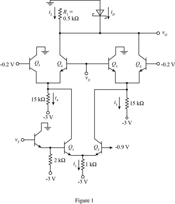
The given diagram is shown in Figure 1.

The expression for the current
Substitute
The expression to determine the value of the current
Substitute
The expression to determine the value of the current
Substitute
The expression for the value of the current
Substitute
The expression to determine the value of the current
Substitute
The output voltage is the voltage of the diode with opposite polarity and is given by,
Conclusion:
Therefore, the value of the current
(b)
The value of the current and voltage
(b)
Answer to Problem 17.15P
The value of the current
Explanation of Solution
Calculation:
The diode
The expression for the current
Substitute
The expression to determine the value of the current
Substitute
The expression to determine the value of the current
Substitute
The expression to determine the value of the current
Substitute
The expression to determine the value of the output voltage is given by,
Substitute
Conclusion:
Therefore, the value of the current
(c)
The value of the current and voltage
(c)
Answer to Problem 17.15P
The value of the current
Explanation of Solution
Calculation:
The transistor
The expression for the current
Substitute
The expression to determine the value of the current
Substitute
The expression to determine the value of the current
Substitute
The diode is in the cut off and the diode current is given by,
The expression to determine the value of the current
Substitute
The expression to determine the value of the output voltage is given by,
Substitute
Conclusion:
Therefore, the value of the current
(d)
The value of the current and voltage
(d)
Answer to Problem 17.15P
The value of the current
Explanation of Solution
Calculation:
The transistor
The expression for the current
Substitute
The expression to determine the value of the current
Substitute
The expression to determine the value of the current
Substitute
The expression for the value of the current
Substitute
The expression to determine the value of the current
Substitute
The output voltage is the voltage of the opposite polarity and is given by,
Conclusion:
Therefore, the value of the current
Want to see more full solutions like this?
Chapter 17 Solutions
MICROELECT. CIRCUIT ANALYSIS&DESIGN (LL)
- Two PCM encoders, PCMI is used to encode a signal which has maximum frequency of 8 kHz and has 150 voltage levels, while PCM2 is used to encode a signal with maximum frequency of 12.8 kHz and 29 voltage levels. Find the bit rate at the output of each encoder. then apply bit multiplexing and find the bit rate at the output of the multiplexer.arrow_forwardNO AI PLEASEarrow_forwardA DPSK has the following data input: d(n) =101011010001 1. Find the output coded sequence and the carrier phase. 2. Recover the input data from the output coded sequence.arrow_forward
- I need help with this problem and an step by step explanation of the solution from the image described below. (Introduction to Signals and Systems)arrow_forwardi need help insolving the following question pleasearrow_forwardI need help with this problem and an step by step explanation of the solution from the image described below. (Introduction to Signals and Systems)arrow_forward
- i need help insolving the following question pleasearrow_forwardNote that all capacitors are large so that their impedance is negligible at signal frequencies of interest. npn equations active Ic Ise VBE/VT = IB = (Is/B)eVB VBE/VT IE = (Is/α)еVB VBE/VT Ic=ẞIB_IС = αIE B α α = B = B+1 1-α Ic α Im Υπ re To= VT 9m Im 550 VAarrow_forwardi need help insolving the following question pleasearrow_forward
 Introductory Circuit Analysis (13th Edition)Electrical EngineeringISBN:9780133923605Author:Robert L. BoylestadPublisher:PEARSON
 Delmar's Standard Textbook Of ElectricityElectrical EngineeringISBN:9781337900348Author:Stephen L. HermanPublisher:Cengage Learning
 Programmable Logic ControllersElectrical EngineeringISBN:9780073373843Author:Frank D. PetruzellaPublisher:McGraw-Hill Education
 Fundamentals of Electric CircuitsElectrical EngineeringISBN:9780078028229Author:Charles K Alexander, Matthew SadikuPublisher:McGraw-Hill Education
 Electric Circuits. (11th Edition)Electrical EngineeringISBN:9780134746968Author:James W. Nilsson, Susan RiedelPublisher:PEARSON
 Engineering ElectromagneticsElectrical EngineeringISBN:9780078028151Author:Hayt, William H. (william Hart), Jr, BUCK, John A.Publisher:Mcgraw-hill Education,


