Fundamentals of Electric Circuits
6th Edition
ISBN: 9780078028229
Author: Charles K Alexander, Matthew Sadiku
Publisher: McGraw-Hill Education
expand_more
expand_more
format_list_bulleted
Videos
Textbook Question
Chapter 8, Problem 33P
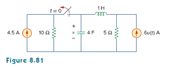
Find v(t) for t > 0 in the circuit of Fig. 8.81.
Expert Solution & Answer
Want to see the full answer?
Check out a sample textbook solution
Students have asked these similar questions
A3 m long cantilever ABC is built-in at A, partially supported at B, 2 m from A,
with a force of 10 kN and carries a vertical load of 20 kN at C. A uniformly distributed
bad of 5 kN/m is also applied between A and B. Determine
(a) the values of the vertical reaction and built-in moment at A and
(b) the deflection of the free end C of the cantilever,
Develop an expression for the slope of the beam at any position and hence plot a slope diagram.
E = 208GN / (m ^ 2) and 1 = 24 * 10 ^ - 6 * m ^ 4
7. Consider the following feedback system with a proportional controller.
K
G(s)
The plant transfer function is given by
G(s) =
10
(s + 2)(s + 10)
You want the system to have a damping ratio of 0.3 for unit step response. What is the
value of K you need to choose to achieve the desired damping ratio? For that value of
K, find the steady-state error for ramp input and settling time for step input.
Hint: Sketch the root locus and find the point in the root locus that intersects with z =
0.3 line.
Create the PLC ladder logic diagram
for the logic gate circuit displayed in
Figure 7-35. The pilot light red (PLTR)
output section has three inputs: PBR,
PBG, and SW. Pushbutton red (PBR)
and pushbutton green (PBG) are inputs
to an XOR logic gate. The output of the
XOR logic gate and the inverted switch
SW) are inputs to a two-input AND
logic gate. These inputs generate the
pilot light red (PLTR) output.
The two-input AND logic gate output
is also fed into a two-input NAND logic
PBR
PBG
SW
TSW
PLTR
Figure 7-35. Logic gate circuit for Example 7-3.
PLTW
Goodheart-Willcox Publisher
gate. The temperature switch (TSW) is the other input to the NAND logic gate. The output generated from
the NAND logic gate is labeled pilot light white (PLTW).
Chapter 8 Solutions
Fundamentals of Electric Circuits
Ch. 8.2 - The switch in Fig. 8.4 was open for a long time...Ch. 8.2 - For the circuit in Fig. 8.7, find: (a) iL(0+),...Ch. 8.3 - If R = 10 , L = 5 H, and C = 2 mF in Fig. 8.8,...Ch. 8.3 - The circuit in Fig. 8.12 has reached steady state...Ch. 8.4 - In Fig. 8.13, let R = 2 , L = 0.4 H, C = 25 mF,...Ch. 8.4 - Refer to the circuit in Fig. 8.17. Find v(t) for t...Ch. 8.5 - Having been in position a for a long time, the...Ch. 8.6 - Find i(t) and v(t) for t 0 in the circuit of Fig....Ch. 8.7 - Determine v and i for t 0 in the circuit of Fig....Ch. 8.7 - For t 0, obtain v0(t) in the circuit of Fig....
Ch. 8.8 - In the op amp circuit shown in Fig. 8.34, vs =...Ch. 8.9 - Find i(t) using PSpice for 0 t 4 s if the pulse...Ch. 8.9 - Refer to the circuit in Fig. 8.21 (see Practice...Ch. 8.10 - Draw the dual circuit of the one in Fig. 8.46.Ch. 8.10 - For the circuit in Fig. 8.50, obtain the dual...Ch. 8.11 - In Fig. 8.52, find the capacitor voltage vC for t ...Ch. 8.11 - The output of a D/A converter is shown in Fig....Ch. 8 - For the circuit in Fig. 8.58, the capacitor...Ch. 8 - For Review Questions 8.1 and 8.2. 8.2For the...Ch. 8 - When a step input is applied to a second-order...Ch. 8 - If the roots of the characteristic equation of an...Ch. 8 - In a series RLC circuit, setting R = 0 will...Ch. 8 - Prob. 6RQCh. 8 - Refer to the series RLC circuit in Fig. 8.59. What...Ch. 8 - Consider the parallel RLC circuit in Fig. 8.60....Ch. 8 - Match the circuits in Fig. 8.61 with the following...Ch. 8 - Prob. 10RQCh. 8 - For the circuit in Fig. 8.62, find: (a)i(0+) and...Ch. 8 - Using Fig. 8.63, design a problem to help other...Ch. 8 - Refer to the circuit shown in Fig. 8.64....Ch. 8 - In the circuit of Fig. 8.65, find: (a) v(0+) and...Ch. 8 - Refer to the circuit in Fig. 8.66. Determine: (a)...Ch. 8 - In the circuit of Fig. 8.67, find: (a) vR(0+) and...Ch. 8 - A series RLC circuit has R = 20 k, L = 0.2 mH, and...Ch. 8 - Design a problem to help other students better...Ch. 8 - The current in an RLC circuit is described by...Ch. 8 - The differential equation that describes the...Ch. 8 - Prob. 11PCh. 8 - If R = 50 , L = 1.5 H, what value of C will make...Ch. 8 - For the circuit in Fig. 8.68, calculate the value...Ch. 8 - The switch in Fig. 8.69 moves from position A to...Ch. 8 - The responses of a series RLC circuit are...Ch. 8 - Find i(t) for t 0 in the circuit of Fig. 8.70....Ch. 8 - In the circuit of Fig. 8.71, the switch...Ch. 8 - Find the voltage across the capacitor as a...Ch. 8 - Obtain v(t) for t 0 in the circuit of Fig. 8.73....Ch. 8 - The switch in the circuit of Fig. 8.74 has been...Ch. 8 - Calculate v(t) for t 0 in the circuit of Fig....Ch. 8 - Assuming R = 2 k, design a parallel RLC circuit...Ch. 8 - For the network in Fig. 8.76, what value of C is...Ch. 8 - The switch in Fig. 8.77 moves from position A to...Ch. 8 - Using Fig. 8.78, design a problem to help other...Ch. 8 - The step response of an RLC circuit is given by...Ch. 8 - Prob. 27PCh. 8 - A series RLC circuit is described by...Ch. 8 - Solve the following differential equations subject...Ch. 8 - Prob. 30PCh. 8 - Consider the circuit in Fig. 8.79. Find vL(0+) and...Ch. 8 - For the circuit in Fig. 8.80, find v(t) for t 0.Ch. 8 - Find v(t) for t 0 in the circuit of Fig. 8.81.Ch. 8 - Calculate i(t) for t 0 in the circuit of Fig....Ch. 8 - Using Fig. 8.83, design a problem to help other...Ch. 8 - Obtain v(t) and i(t) for t 0 in the circuit of...Ch. 8 - For the network in Fig. 8.85, solve for i(t) for t...Ch. 8 - Refer to the circuit in Fig. 8.86. Calculate i(t)...Ch. 8 - Determine v(t) for t 0 in the circuit of Fig....Ch. 8 - The switch in the circuit of Fig. 8.88 is moved...Ch. 8 - For the network in Fig. 8.89, find i(t) for t 0....Ch. 8 - Given the network in Fig. 8.90, find v(t) for t ...Ch. 8 - The switch in Fig. 8.91 is opened at t = 0 after...Ch. 8 - A series RLC circuit has the following parameters:...Ch. 8 - In the circuit of Fig. 8.92, find v(t) and i(t)...Ch. 8 - Prob. 46PCh. 8 - Find the output voltage vo(t) in the circuit of...Ch. 8 - Given the circuit in Fig. 8.95, find i(t) and v(t)...Ch. 8 - Determine i(t) for t 0 in the circuit of Fig....Ch. 8 - For the circuit in Fig. 8.97, find i(t) for t 0....Ch. 8 - Find v(t) for t 0 in the circuit of Fig. 8.98....Ch. 8 - The step response of a parallel RLC circuit is...Ch. 8 - After being open for a day, the switch in the...Ch. 8 - Using Fig. 8.100, design a problem to help other...Ch. 8 - For the circuit in Fig. 8.101, find v(t) for t 0....Ch. 8 - In the circuit of Fig. 8.102, find i(t) for t 0....Ch. 8 - Given the circuit shown in Fig. 8.103, determine...Ch. 8 - In the circuit of Fig. 8.104, the switch has been...Ch. 8 - The switch in Fig. 8.105 has been in position 1...Ch. 8 - Obtain i1 and i2 for t 0 in the circuit of Fig....Ch. 8 - For the circuit in Prob. 8.5, find i and v for t ...Ch. 8 - Find the response vR(t) for t 0 in the circuit of...Ch. 8 - For the op amp circuit in Fig. 8.108, find the...Ch. 8 - Using Fig. 8.109, design a problem to help other...Ch. 8 - Determine the differential equation for the op amp...Ch. 8 - Obtain the differential equations for vo(t) in the...Ch. 8 - In the op amp circuit of Fig. 8.112, determine...Ch. 8 - For the step function vs = u(t), use PSpice or...Ch. 8 - Given the source-free circuit in Fig. 8.114, use...Ch. 8 - For the circuit in Fig. 8.115, use PSpice or...Ch. 8 - Obtain v(t) for 0 t 4 s in the circuit of Fig....Ch. 8 - The switch in Fig. 8.117 has been in position 1...Ch. 8 - Design a problem, to be solved using PSpice or...Ch. 8 - Draw the dual of the circuit shown in Fig. 8.118.Ch. 8 - Obtain the dual of the circuit in Fig. 8.119.Ch. 8 - Find the dual of the circuii in Fig. 8.120.Ch. 8 - Draw the dual of the circuit in Fig. 8.121.Ch. 8 - An automobile airbag igniter is modeled by the...Ch. 8 - A load is modeled as a 100-mH inductor in parallel...Ch. 8 - A mechanical system is modeled by a series RLC...Ch. 8 - An oscillogram can be adequately modeled by a...Ch. 8 - The circuit in Fig. 8.123 is the electrical analog...Ch. 8 - Figure 8.124 shows a typical tunnel-diode...
Additional Engineering Textbook Solutions
Find more solutions based on key concepts
Which of the following are illegal variable names in Python, and why? x 99bottles july2009 theSalesFigureForFis...
Starting Out with Python (4th Edition)
This optional Google account security feature sends you a message with a code that you must enter, in addition ...
SURVEY OF OPERATING SYSTEMS
The job of the _____ is to fetch instructions, carry out the operations commanded by the instructions, and prod...
Starting Out With Visual Basic (8th Edition)
The solid steel shaft AC has a diameter of 25 mm and is supported by smooth bearings at D and E. It is coupled ...
Mechanics of Materials (10th Edition)
Assume a telephone signal travels through a cable at two-thirds the speed of light. How long does it take the s...
Electric Circuits. (11th Edition)
Comprehension Check 7-14
The power absorbed by a resistor can be given by P = I2R, where P is power in units of...
Thinking Like an Engineer: An Active Learning Approach (4th Edition)
Knowledge Booster


Learn more about
Need a deep-dive on the concept behind this application? Look no further. Learn more about this topic, electrical-engineering and related others by exploring similar questions and additional content below.Similar questions
- Imaginary Axis (seconds) 1 6. Root locus for a closed-loop system with L(s) = is shown below. s(s+4)(s+6) 15 10- 0.89 0.95 0.988 0.988 -10 0.95 -15 -25 0.89 20 Root Locus 0.81 0.7 0.56 0.38 0.2 5 10 15 System: sys Gain: 239 Pole: -0.00417 +4.89 Damping: 0.000854 Overshoot (%): 99.7 Frequency (rad/s): 4.89 System: sys Gain: 16.9 Pole: -1.57 Damping: 1 Overshoot (%): 0 Frequency (rad/s): 1.57 0.81 0.7 0.56 0.38 0.2 -20 -15 -10 -5 5 10 Real Axis (seconds) From the values shown in the figure, compute the following. a) Range of K for which the closed-loop system is stable. b) Range of K for which the closed-loop step response will not have any overshoot. Note that when all poles are real, the step response has no overshoot. c) Smallest possible peak time of the system. Note that peak time is the smallest when wa is the largest for the dominant pole. d) Smallest possible settling time of the system. Note that peak time is the smallest when σ is the largest for the dominant pole.arrow_forwardFor a band-rejection filter, the response drops below this half power point at two locations as visualised in Figure 7, we need to find these frequencies. Let's call the lower frequency-3dB point as fr and the higher frequency -3dB point fH. We can then find out the bandwidth as f=fHfL, as illustrated in Figure 7. 0dB Af -3 dB Figure 7. Band reject filter response diagram Considering your AC simulation frequency response and referring to Figure 7, measure the following from your AC simulation. 1% accuracy: (a) Upper-3db Frequency (fH) = Hz (b) Lower-3db Frequency (fL) = Hz (c) Bandwidth (Aƒ) = Hz (d) Quality Factor (Q) =arrow_forwardP 4.4-21 Determine the values of the node voltages V1, V2, and v3 for the circuit shown in Figure P 4.4-21. 29 ww 12 V +51 Aia ww 22. +21 ΖΩ www ΖΩ w +371 ①1 1 Aarrow_forward
- 1. What is the theoretical attenuation of the output voltage at the resonant frequency? Answer to within 1%, or enter 0, or infinity (as “inf”) Attenuation =arrow_forwardWhat is the settling time for your output signal (BRF_OUT)? For this question, We define the settling time as the period of time it has taken for the output to settle into a steady state - ie when your oscillation first decays (aka reduces) to less than approximately 1/20 (5%) of the initial value. (a) Settling time = 22 μs Your last answer was interpreted as follows: Incorrect answer. Check 22 222 What is the peak to peak output voltage (BRF_OUT pp) at the steady state condition? You may need to use the zoom function to perform this calculation. Select a time point that is two times the settling time you answered in the question above. Answer to within 10% accuracy. (a) BRF_OUT pp= mVpp As you may have noticed, the output voltage amplitude is a tiny fraction of the input voltage, i.e. it has been significantly attenuated. Calculate the attenuation (decibels = dB) in the output signal as compared to the input based on the formula given below. Answer to within 1% accuracy.…arrow_forwardmy previous answers for a,b,d were wrong a = 1050 b = 950 d=9.99 c was the only correct value i got previously c = 100hz is correctarrow_forward
- V₁(t) ww ZRI ZLI ZL2 ZTH Zci VTH Zc21 Figure 8. Circuit diagram showing calculation approach for VTH and Z TH we want to create a blackbox for the red region, we want to use the same input signal conditions as previously the design of your interference ector circuit: Sine wave with a 1 Vpp, with a frequency of 100 kHz (interference) Square wave with 2.4Vpp, with a frequency of 10 kHz (signal) member an AC Thevenin equivalent is only valid at one frequency. We have chosen to calculate the Thevenin equivalent circuit (and therefore the ackbox) at the interference frequency (i.e. 100 kHz), and the signal frequency (i.e. 10 kHz) as these are the key frequencies to analyse. Your boss is assured you that the waveform converter module has been pre-optimised to the DAB Receiver if you use the recommended circuit topology.arrow_forwardVs(t) + v(t) + vi(t) ZR ZL Figure 1: Second order RLC circuit Zc + ve(t) You are requested to design the circuit shown in Figure 1. The circuit is assumed to be operating at its resonant frequency when it is fed by a sinusoidal voltage source Vs (t) = 2sin(le6t). To help design your circuit you have been given the value of inductive reactance ZL = j1000. Assume that the amplitude of the current at resonance is Is (t) = 2 mA. Based on this information, answer the following to help design your circuit. Use cartesian notation for your answers, where required.arrow_forwardWhat is the attenuation at the resonant frequency? You should use the LTSpice cursors for your measurement. Answer to within 1% accuracy, or enter 0, or infinity (as "inf") (a) Attenuation (dB) = dB Check You may have noticed that it was significantly easier to use frequency-domain "AC" simulation to measure the attenuation, compared to the steps we performed in the last few questions. (i.e. via a time-domain "transient" simulation). AC analysis allows us to observe and quantify large scale positive or negative changes in a signal of interest across a wide range of different frequencies. From the response you will notice that only frequencies that are relatively close to 100 kHz have been attenuated. This is the result of the Band-reject filter you have designed, and shows the 'rejection' (aka attenuation) of any frequencies that lie in a given band. The obvious follow-up question is how do we define this band? We use a quantity known as the bandwidth. A commonly used measurement for…arrow_forward
- V₁(t) ww ZRI ZLI ZL2 ZTH Zci VTH Zc21 Figure 8. Circuit diagram showing calculation approach for VTH and Z TH we want to create a blackbox for the red region, we want to use the same input signal conditions as previously the design of your interference ector circuit: Sine wave with a 1 Vpp, with a frequency of 100 kHz (interference) Square wave with 2.4Vpp, with a frequency of 10 kHz (signal) member an AC Thevenin equivalent is only valid at one frequency. We have chosen to calculate the Thevenin equivalent circuit (and therefore the ackbox) at the interference frequency (i.e. 100 kHz), and the signal frequency (i.e. 10 kHz) as these are the key frequencies to analyse. Your boss is assured you that the waveform converter module has been pre-optimised to the DAB Receiver if you use the recommended circuit topology.arrow_forwardVs(t) + v(t) + vi(t) ZR ZL Figure 1: Second order RLC circuit Zc + ve(t) You are requested to design the circuit shown in Figure 1. The circuit is assumed to be operating at its resonant frequency when it is fed by a sinusoidal voltage source Vs (t) = 2sin(le6t). To help design your circuit you have been given the value of inductive reactance ZL = j1000. Assume that the amplitude of the current at resonance is Is (t) = 2 mA. Based on this information, answer the following to help design your circuit. Use cartesian notation for your answers, where required.arrow_forwardFor a band-rejection filter, the response drops below this half power point at two locations as visualised in Figure 7, we need to find these frequencies. Let's call the lower frequency-3dB point as fr and the higher frequency -3dB point fH. We can then find out the bandwidth as f=fHfL, as illustrated in Figure 7. 0dB Af -3 dB Figure 7. Band reject filter response diagram Considering your AC simulation frequency response and referring to Figure 7, measure the following from your AC simulation. 1% accuracy: (a) Upper-3db Frequency (fH) = Hz (b) Lower-3db Frequency (fL) = Hz (c) Bandwidth (Aƒ) = Hz (d) Quality Factor (Q) =arrow_forward
arrow_back_ios
SEE MORE QUESTIONS
arrow_forward_ios
Recommended textbooks for you
 Introductory Circuit Analysis (13th Edition)Electrical EngineeringISBN:9780133923605Author:Robert L. BoylestadPublisher:PEARSON
 Delmar's Standard Textbook Of ElectricityElectrical EngineeringISBN:9781337900348Author:Stephen L. HermanPublisher:Cengage Learning
 Programmable Logic ControllersElectrical EngineeringISBN:9780073373843Author:Frank D. PetruzellaPublisher:McGraw-Hill Education
 Fundamentals of Electric CircuitsElectrical EngineeringISBN:9780078028229Author:Charles K Alexander, Matthew SadikuPublisher:McGraw-Hill Education
 Electric Circuits. (11th Edition)Electrical EngineeringISBN:9780134746968Author:James W. Nilsson, Susan RiedelPublisher:PEARSON
 Engineering ElectromagneticsElectrical EngineeringISBN:9780078028151Author:Hayt, William H. (william Hart), Jr, BUCK, John A.Publisher:Mcgraw-hill Education,
Introductory Circuit Analysis (13th Edition)
Electrical Engineering
ISBN:9780133923605
Author:Robert L. Boylestad
Publisher:PEARSON
Delmar's Standard Textbook Of Electricity
Electrical Engineering
ISBN:9781337900348
Author:Stephen L. Herman
Publisher:Cengage Learning
Programmable Logic Controllers
Electrical Engineering
ISBN:9780073373843
Author:Frank D. Petruzella
Publisher:McGraw-Hill Education
Fundamentals of Electric Circuits
Electrical Engineering
ISBN:9780078028229
Author:Charles K Alexander, Matthew Sadiku
Publisher:McGraw-Hill Education
Electric Circuits. (11th Edition)
Electrical Engineering
ISBN:9780134746968
Author:James W. Nilsson, Susan Riedel
Publisher:PEARSON
Engineering Electromagnetics
Electrical Engineering
ISBN:9780078028151
Author:Hayt, William H. (william Hart), Jr, BUCK, John A.
Publisher:Mcgraw-hill Education,
L21E127 Control Systems Lecture 21 Exercise 127: State-space model of an electric circuit; Author: bioMechatronics Lab;https://www.youtube.com/watch?v=sL0LtyfNYkM;License: Standard Youtube License