Concept explainers
Videos
In the circuit of Fig. 7.140, find vo and io, given that vs = 10[1 – e–t]u(t) V.
![Chapter 7, Problem 75P, In the circuit of Fig. 7.140, find vo and io, given that vs = 10[1 et]u(t) V.](http://dev-ingestion-image-output.s3-website-us-east-1.amazonaws.com/9780078028229/Chapter-7/images/28229-7-75p-question-digital_image_001.png)
Find the output voltage
Answer to Problem 75P
The output voltage
Explanation of Solution
Given data:
Refer to Figure 7.140 in the textbook.
The value of capacitance
The source voltage
Formula used:
Write the general expression for the unit step function.
Calculation:
The given Figure 7.140 is redrawn as shown in Figure 1.
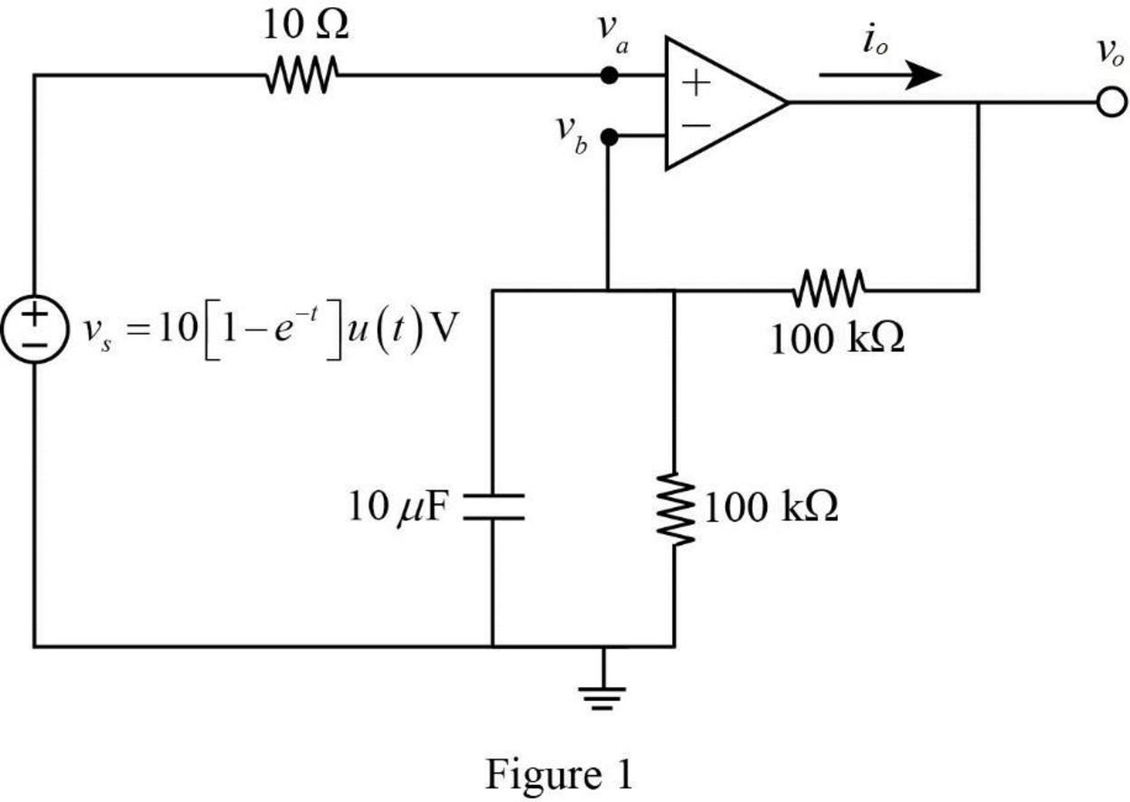
The given source voltage is,
Apply the unit step function in equation (1) to equation (2).
Consider the voltage at the non-inverting terminal as
For
Since the source voltage
For
The voltage,
On differentiating the equation (3).
In Figure 1, apply Kirchhoff’s current law at node
Substitute
Rearrange the equation as follows,
Simplify the equation as follows,
Apply the unit step function in equation (1) to equation (5).
The output current
Substitute
Convert the unit A to
Conclusion:
Thus, the output voltage
Want to see more full solutions like this?
Chapter 7 Solutions
Fundamentals of Electric Circuits


- 1) Find Vo in the following circuit. Assume the mesh currents are clockwise. ΠΩ Ω ΖΩ ww 1Ω ww 24/0° (± 6 Ω j4 Ω 1Ω +arrow_forwardPlease show all stepsarrow_forward11-3) similar to Lathi & Ding, Prob. P.6.8-1 Consider the carrier modulator shown in the figure below, which transmits a binary carrier signal. The baseband generator uses polar NRZ signaling with rectangular pulses. The data rate is 8 Mbit/s. (a) If the modulator generates a binary PSK signal, what is the bandwidth of the modulated output? (b) If the modulator generates FSK with the difference fel - fco = 6 MHz (cf. Fig 6.32c), determine the modulated signal bandwidth. Binary data source Baseband signal generator Modulated output Modulator N-E---arrow_forward
- Choose the best answer for each: 1. What does SRAM use to store data? 。 a) Capacitors ob) Latches 。 c) Flip-flops od) Transistors 2. Which RAM type requires refreshing? o a) SRAM ob) DRAM 。 c) ROM od) Flash 3. What type of memory retains data only while power is on? a) ROM 。 b) EEPROM o c) DRAM od) Flash 4. How many addresses can a 15-bit address bus handle? o a) 32k • b) 64k o c) 16k od) lk 5. What operation occurs when data is copied out of memory without erasing? oa) Write ob) Read o c) Refresh o d) Load 6. DRAM cells store bits using: a) Flip-flops 。 b) Capacitors c) Diodes od) Resistors 7. The cache located inside the CPU is: 。 a) L2 cache o b) LI cache °c) ROM od) HDD 8. SDRAM is synchronized with: o a) Cache ob) Data Bus c) System Clock od) Hard Disk 9. The bus that carries commands is called: o a) Data Bus b) Control Bus o c) Address Bus o d) Logic Bus 10. What is the main use of SRAM? o Disk storage o Cache o Main memory o Registers 11. The smallest addressable unit in…arrow_forwardQ4: A cache memory is 128k × 16. How many bytes can it store?arrow_forwardSketch the output of the analogue computer shown below and find its closest describing function [suppose any variable to find the DF] +1 ew2 HI e2 1.0 +21 LO SJ eo SJ ew LO 1.0 +|e1| HI -1 ew1 ek(1 + e。) |e1| k = 1+|e1| Figure V-5 Feedback Limiter Behavior ROUNDED, DUE TO DIODE NONLINEARITY LIMIT VOLTAGE 409 DIODE CONDUCTS First, write the output transaction, then draw the output wave, and then find the Describing function. I need to solve the question step by step, with an explanation of each step.arrow_forward
- Sketch the output of the analogue computer shown below and find its closest describing function [suppose any variable to find the DF] SJ ew2 ew₁ HI |e2| 2 LO 1.0 +21 LO -1 HI Jel 1.0+|e1| ROUNDED, DUE TO DODE NONLINEARITY LIMIT VOLTAGE DIODE CONDUCTS ew1e, -k(1+ e。) k = |e1| 1+|e1| Figure 1-5 Feedback Limiter Behavior First, write the output transaction, then draw the output wave, and then find the Describing function. I need to solve the question step by step, with an explanation of each step.arrow_forwardSketch the output of the analogue computer shown below and find its closest describing function [suppose any variable to find the DF] SJ +1 HI LO e2 1.0 +21 ew2 eo SJ ew₁ LO Jel 1.0 +|e1| HI -1 ew1 ek(1+eo) k = |e1| 1+|e1| First, write the output transaction, then draw the output wave, and then find the Describing function. I need to solve the question step by step, with an explanation of each step.arrow_forwardCan you help me find the result of an integral 0/2 a² X + a dxarrow_forward
 Introductory Circuit Analysis (13th Edition)Electrical EngineeringISBN:9780133923605Author:Robert L. BoylestadPublisher:PEARSON
 Delmar's Standard Textbook Of ElectricityElectrical EngineeringISBN:9781337900348Author:Stephen L. HermanPublisher:Cengage Learning
 Programmable Logic ControllersElectrical EngineeringISBN:9780073373843Author:Frank D. PetruzellaPublisher:McGraw-Hill Education
 Fundamentals of Electric CircuitsElectrical EngineeringISBN:9780078028229Author:Charles K Alexander, Matthew SadikuPublisher:McGraw-Hill Education
 Electric Circuits. (11th Edition)Electrical EngineeringISBN:9780134746968Author:James W. Nilsson, Susan RiedelPublisher:PEARSON
 Engineering ElectromagneticsElectrical EngineeringISBN:9780078028151Author:Hayt, William H. (william Hart), Jr, BUCK, John A.Publisher:Mcgraw-hill Education,