Concept explainers
Videos
Obtain the inductor current for both t < 0 and t > 0 in each of the circuits in Fig. 7.120.
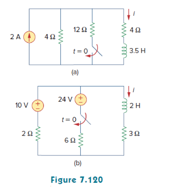
(a)
Calculate the value of inductor current
Answer to Problem 54P
The value of inductor current
Explanation of Solution
Given data:
Refer to Figure 7.120 in the textbook.
The value of inductance L in Figure 7.120(a) is
Formula used:
Write the general expression to find the complete response of current for the RL circuit.
Here,
Write the expression to calculate the time constant for the RL circuit.
Here,
L is the inductance of the inductor.
Calculation:
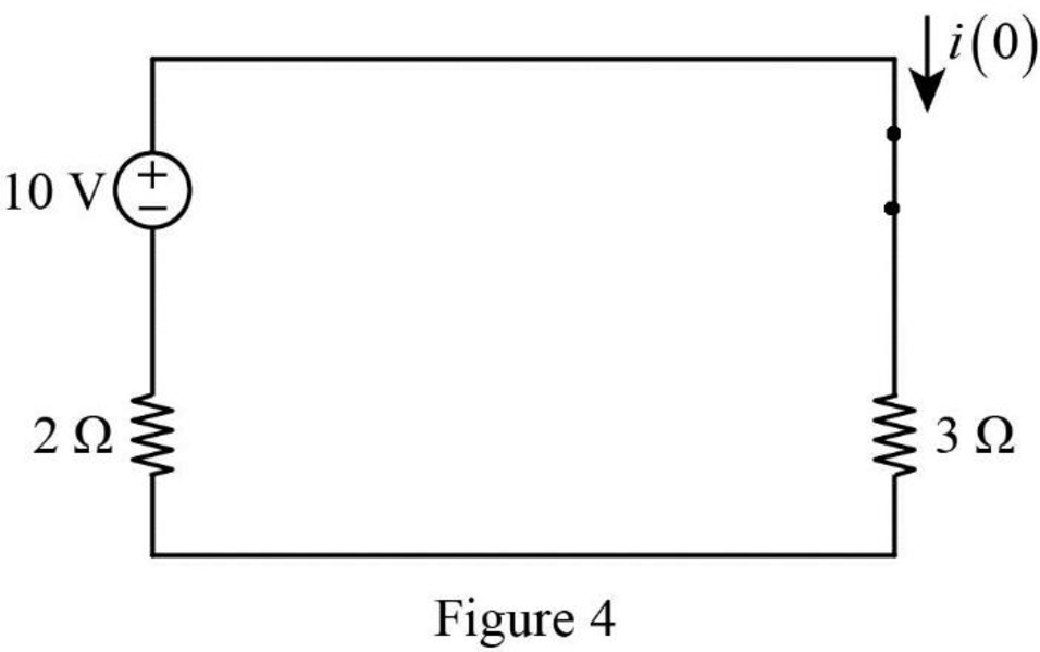
Figure 1 shows the modified circuit diagram when
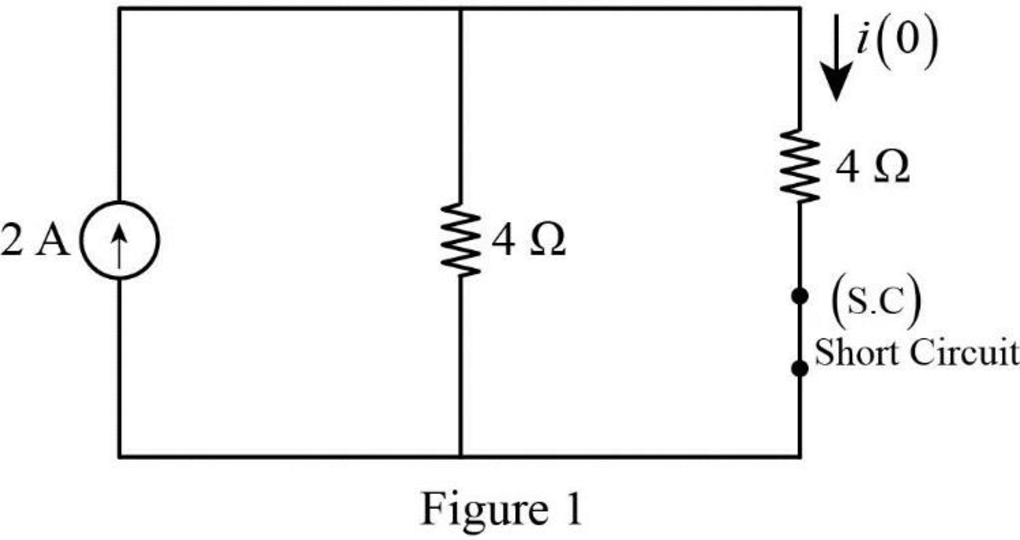
In Figure 1, the switch is kept in open position for all
Therefore, the inductor current
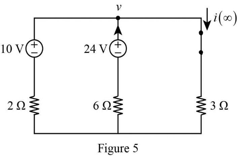
Figure 2 shows the modified circuit diagram when the switch is kept in close position for all
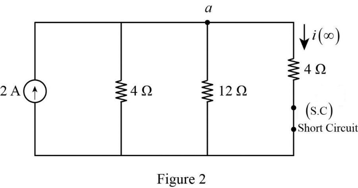
Apply Kirchhoff’s current law at node a.
Rearrange the equation as follows,
The final inductor current
Substitute
Figure 3 shows the equivalent resistance at the inductor terminal.
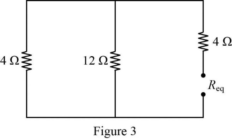
In Figure 3, the equivalent resistance is calculated as follows.
Substitute
Substitute the units
Substitute
Therefore, the inductor current
Conclusion:
Thus, the value of inductor current
(b)
Calculate the value of inductor current
Answer to Problem 54P
The value of inductor current
Explanation of Solution
Given data:
Refer to Figure 7.120 in the textbook.
The value of inductance L in Figure 7.120(b) is
Calculation:
Figure 4 shows the modified circuit diagram when switch is kept open for a long time at
In Figure 4,
Rearrange the equation as follows,
Therefore, the inductor current
Figure 5 shows the redrawn circuit when switch is kept in closed position at
In Figure 5, apply Kirchhoff’s current law at node v.
Rearrange the equation as follows,
The final inductor current
Substitute
Figure 6 shows the equivalent resistance at the inductor terminal.
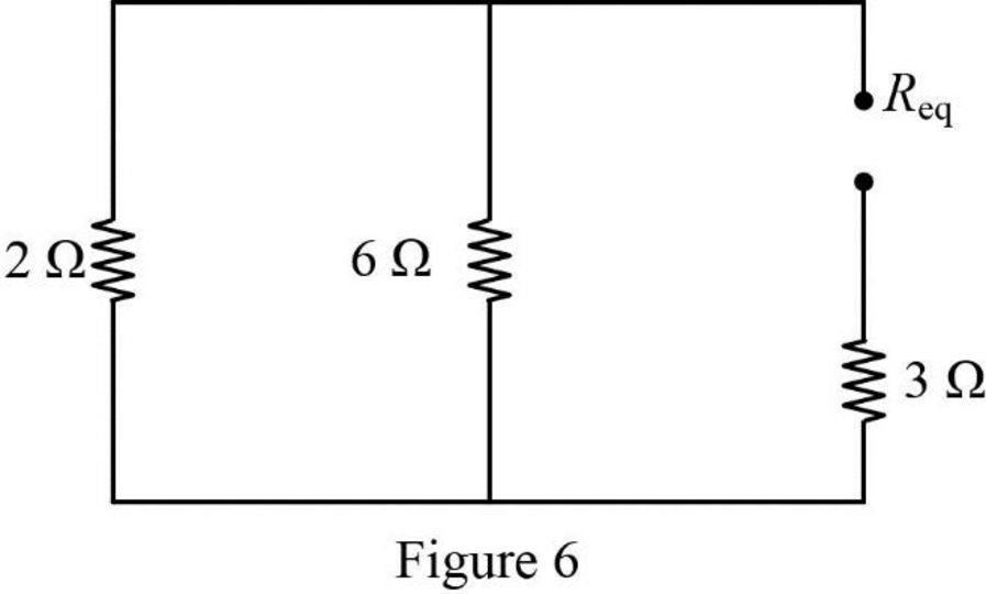
In Figure 6, the equivalent resistance is calculated as follows.
Substitute
Substitute the units
Substitute
Therefore, the inductor current
Conclusion:
Thus, the value of inductor current
Want to see more full solutions like this?
Chapter 7 Solutions
Fundamentals of Electric Circuits


- can you show the steps to answer question.arrow_forwardQ2. Figure Q2 shows a block diagram with an input of C(s) and an output R(s). a) C(s) K₁ R(s) K2 1 + 5s 1+2s Figure Q2. Block diagram of control system. Simply the block diagram to get the transfer function of the system C(s)/R(s). b) What is the order of the system? c) What is the gain of the system? d) Determine the values of K₁ and K₂ to obtain a natural frequency w of 0.5 rad/s and damping ratio of 0.4. e) What is the rise time and overshoot of the system with a unit step input?arrow_forwardQ4. a) A purely derivative controller (i.e. with a zero at the origin only) is defined by an improper transfer function. Considering its asymptotic behaviour, explain why a purely derivative controller is difficult to implement in practice. Relate your explanation to the potential limitations on system performance. b) Discuss the potential issues faced by a control system with a large cut-off frequency. Relate your discussion to the implications on system performance. c) The transfer function of a lag compensator is given by 2 KPID(S) = 2.2++0.2s S By using the asymptotic approximation technique: (i) Obtain the standard form and corner frequency for each individual component of KPID(S). (ii) Clearly describe the asymptotic behaviour of each individual component of KPID(S).arrow_forward
- Module Code: EN2058 Q1. a) List the advantages and disadvantages of a closed loop system compared to an open loop system. b) c) What is the procedure for designing a control system for a bread toaster? An RC circuit is given in Figure Q1. vi(t) and v(t) are the input and output voltages. (i) Derive the transfer function of the circuit. (ii) With a unit step change vi(t) applied to the circuit, derive and sketch the time response of the circuit. R1 R2 v₁(t) R3 C1 vo(t) R₁ =R2 = 10 k R3 = 100 kn C₁ = 100 μF Figure Q1. RC circuit. (iii) Assuming zero initial conditions, obtain the impulse and ramp responses of the circuit from the step response derived in (ii). Sketching is not needed.arrow_forwardQ3. a) The frequency response method enables the study of the steady-state response of a system G(s). What type of inputs are used for frequency response? If the system is linear and stable, how does the output differ from the input? Compare the main characteristics of two types frequency response plots. b) Consider the control system shown in Figure Q3. Controller E(s) R(s) Desired output C(s) Plant G(s) Y(s) Actual output 3(s + 3) C(s) = k G(s) = = s(s - 1)(s + 10) Figure Q3. Closed-loop system. (i) Considering definitions in the study of bounded-input bounded-output stability, is G(s) stable? Classify the poles and zeros of G(s). (ii) G(s) defined in Figure Q3 is a system completely characterised by its transfer function. Explain why this is the case. (iii) Obtain the closed-loop transfer function P(s) = Y(s)/R(s) of the system. (iv) Based on your result for the previous question [Question 3b)-(iii)], use the Routh-Hurwitz stability criterion to determine suitable values of gain K…arrow_forwardPlease, I want the solution in two ways: Method 1 (without the Smith chart): Method 2 (using the Smith chart): A short circuit stub of length 0.04λ is used to match a 50 Ω lossless line to a load ZL = RL + j30 Ω. Use Smith chart to find:(a) The distance between the stub and the load.(b) The value of RL .arrow_forward
- THE FIRST PAGE OF THIS QUESTION SECTION BELOW IS THE FIRST IMAGE UPLOADED, WHICH SHOWS A digital synchronous sequential circuit and then comes the questions below:1B) Suppose the flip-flops are 74F74 devices and the AND gates are 74F08 devices. Let maxtpd,D=9ns, maxtsu,D=3ns, and maxtpd,AND=6ns. What is the maximum clock frequency at which the circuit can operate reliably? 2) Compare serial transmission and parallel transmission and discuss their advantages and disadvantages. 3) Explain briefly how the slave can protect itself from being overwhelmed by the master in I2 4) A hypothetical logic family has the following specifications. VOH=4.6V VIH=4.0V VOL=0.5V VIL=1.0V IOH=-1mA IIH=50μA IOL=8mA IIL=-0.6mA (4a) What are the noise margins? (4b) What is the fan-out capability?…arrow_forwardTHE FIRST PAGE OF THIS QUESTION SECTION BELOW IS THE FIRST IMAGE UPLOADED, WHICH SHOWS A digital synchronous sequential circuit and then comes the questions below:1B) Suppose the flip-flops are 74F74 devices and the AND gates are 74F08 devices. Let maxtpd,D=9ns, maxtsu,D=3ns, and maxtpd,AND=6ns. What is the maximum clock frequency at which the circuit can operate reliably? 2) Compare serial transmission and parallel transmission and discuss their advantages and disadvantages. 3) Explain briefly how the slave can protect itself from being overwhelmed by the master in I2 4) A hypothetical logic family has the following specifications. VOH=4.6V VIH=4.0V VOL=0.5V VIL=1.0V IOH=-1mA IIH=50μA IOL=8mA IIL=-0.6mA (4a) What are the noise margins? (4b) What is the fan-out capability?…arrow_forwardI need help on this question a) Find y(t) =yh(t) +yp(t) in time domainIs the system over-damped, under-damped, or critical?arrow_forward
- Given f(t)=a sin(ßt) a = 10 & ß = 23 Find the Laplace Transform using the definition F(s) = ∫f(t)e-stdtarrow_forward= Calculate Avf, Zif, and Zof for the amplifier circuit,Assume he = 50, hie 1.1k2, and identical transistors? 150kQ Vs 5002 HH +25v 10k +6 · 47ΚΩ 47k2 4.7k0} 33 ΚΩ 4.7ΚΩ 10k w 4.7kQ HH Voarrow_forwardFor the four-pole filter in Fig. (2), determine the capacitance values required to produce a critical frequency of 2680 Hz if all the resistors in the RC low-pass circuits are 1.8 K. Also select values for the feedback resistors to get a Butterworth response. Note: For a Butterworth response, the damping factor must be 1.848 for the first stage and 0.765 for the second stage. (2) Re Res ww " = 11arrow_forward
 Introductory Circuit Analysis (13th Edition)Electrical EngineeringISBN:9780133923605Author:Robert L. BoylestadPublisher:PEARSON
 Delmar's Standard Textbook Of ElectricityElectrical EngineeringISBN:9781337900348Author:Stephen L. HermanPublisher:Cengage Learning
 Programmable Logic ControllersElectrical EngineeringISBN:9780073373843Author:Frank D. PetruzellaPublisher:McGraw-Hill Education
 Fundamentals of Electric CircuitsElectrical EngineeringISBN:9780078028229Author:Charles K Alexander, Matthew SadikuPublisher:McGraw-Hill Education
 Electric Circuits. (11th Edition)Electrical EngineeringISBN:9780134746968Author:James W. Nilsson, Susan RiedelPublisher:PEARSON
 Engineering ElectromagneticsElectrical EngineeringISBN:9780078028151Author:Hayt, William H. (william Hart), Jr, BUCK, John A.Publisher:Mcgraw-hill Education,