
Concept explainers
Videos
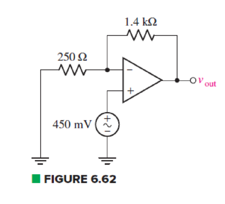
For the circuit of Fig. 6.62, calculate the differential input voltage and the input bias current if the op amp is a(n) (a) μA741; (b) LF411; (c) AD549K.
(a)
Find the differential input voltage and input bias current of op amp.
Answer to Problem 50E
The differential voltage
Explanation of Solution
Given Data:
Differential op amp is
Calculation:
The redrawn circuit of op amp is shown in Figure 1 as follows:
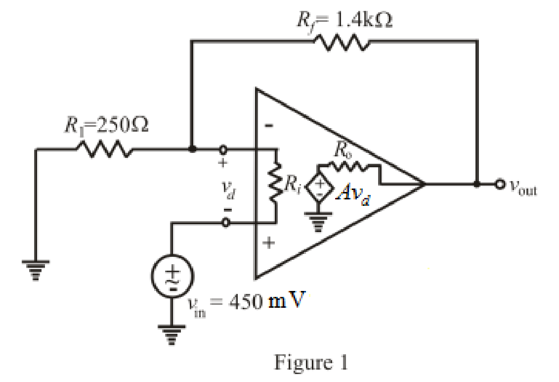
Refer to the redrawn Figure 1:
The expression for the nodal analysis at the nodal voltage
Here,
The expression for nodal analysis at nodal voltage
Here,
The expression for the bias input current of differential op amp is:
Here,
Simplify the equation (1) for
Refer to the TABLE 6.3 in the textbook.
Substitute
Rearrange for
Substitute
Substitute
Substitute
Rearrange for
Conclusion:
Thus, the differential voltage
(b)
Find the differential input voltage and input bias current of op amp.
Answer to Problem 50E
The differential voltage
Explanation of Solution
Given Data:
Differential op amp is
Calculation:
Refer to the TABLE 6.3 in the textbook.
Substitute
Rearrange for
Substitute
Substitute
Substitute
Rearrange for
Conclusion:
Thus, the differential voltage
(c)
Find the differential input voltage and input bias current of
Answer to Problem 50E
The differential voltage
Explanation of Solution
Given Data:
Differential op amp is
Calculation:
Refer to the TABLE 6.3 in the textbook.
Substitute
Rearrange for
Substitute
Substitute
Substitute
Rearrange for
Conclusion:
Thus, the differential voltage
Want to see more full solutions like this?
Chapter 6 Solutions
Loose Leaf for Engineering Circuit Analysis Format: Loose-leaf
Additional Engineering Textbook Solutions
Starting Out with Java: From Control Structures through Objects (7th Edition) (What's New in Computer Science)
BASIC BIOMECHANICS
Database Concepts (8th Edition)
Electric Circuits. (11th Edition)
Concepts Of Programming Languages
Thermodynamics: An Engineering Approach


- Problems A.1 The square-law modulator is a device for the generation of DSB-PC-AM signals. In the square-law modulator, the sum of the modulating signal and the carrier wave forms the input signal to a nonlinear device. The output signal of the nonlinear device is a linear combination of the input signal and the square of the input signal. The output signal of the nonlinear device is then band-pass filtered. The BPF has a center frequency that is the same as the carrier frequency and a bandwidth that is twice the message bandwidth. Show the output of the BPF is a DSB-PC-AM signal, and determine a requirement between the carrier frequency and the message bandwidth that must be satisfied.arrow_forwardGive the current voltage relationship of the D-MOSFET and E-MOSFET.arrow_forwardAnswer A is wrong.arrow_forward
- The part of machine level instruction, which tells the central processor what was to be done is: A. Address B. None of the above C. Operation code D. Operandarrow_forwardWhich of the following statement is TRUE? 1. In RISC processors, each instruction requires only two clock cycles to complete, resulting in consistent execution time 2. RISC has more transistors and fewer registers 3. RISC has more registers and fewer transistorsarrow_forwardDifferentiate between JFET and BJT.arrow_forward
- Give relation between αdc and βdc.arrow_forwardFind the power delivered across the 45 ohm resistorarrow_forwardA half-wave controlled rectifier is supplied by a 230 Vrms voltage source and has load resistance of 2502. Calculate the delay angle a that produces a load-absorbed power of 200W.arrow_forward
- not use ai pleasearrow_forwardFigure 1 shows a half-wave controlled rectifier which is supplied by a Vin = 120 Vrms voltage source. Assume that the load resistance is R = 10 2. Determine: a) The firing angle a of the thyristor to produce an average output voltage 50Vdc. Vin=Vmsinoot b) The average power Po absorbed by the load R. Figure 1 R = 1092arrow_forwardQ1. What is power dissipation in the Zener diode circuit given for a) RL=100 Ohm ? b) RL=∞arrow_forward
 Introductory Circuit Analysis (13th Edition)Electrical EngineeringISBN:9780133923605Author:Robert L. BoylestadPublisher:PEARSON
 Delmar's Standard Textbook Of ElectricityElectrical EngineeringISBN:9781337900348Author:Stephen L. HermanPublisher:Cengage Learning
 Programmable Logic ControllersElectrical EngineeringISBN:9780073373843Author:Frank D. PetruzellaPublisher:McGraw-Hill Education
 Fundamentals of Electric CircuitsElectrical EngineeringISBN:9780078028229Author:Charles K Alexander, Matthew SadikuPublisher:McGraw-Hill Education
 Electric Circuits. (11th Edition)Electrical EngineeringISBN:9780134746968Author:James W. Nilsson, Susan RiedelPublisher:PEARSON
 Engineering ElectromagneticsElectrical EngineeringISBN:9780078028151Author:Hayt, William H. (william Hart), Jr, BUCK, John A.Publisher:Mcgraw-hill Education,