![MindTap Engineering for Glover/Overbye/Sarma's Power System Analysis and Design, 6th Edition, [Instant Access], 1 term (6 months)](https://s3.amazonaws.com/compass-isbn-assets/textbook_empty_images/large_textbook_empty.svg)
MindTap Engineering for Glover/Overbye/Sarma's Power System Analysis and Design, 6th Edition, [Instant Access], 1 term (6 months)
6th Edition
ISBN: 9781305636309
Author: J. Duncan Glover; Thomas Overbye; Mulukutla S. Sarma
Publisher: Cengage Learning US
expand_more
expand_more
format_list_bulleted
Concept explainers
Videos
Textbook Question
Chapter 2, Problem 2.50P
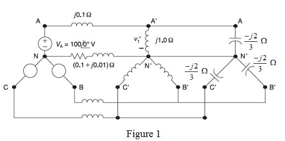
Consider the balanced three-phase system shown in Figure 2.34. Deter mine
Expert Solution & Answer

Trending nowThis is a popular solution!

Students have asked these similar questions
Calculate the voltage gain and I/O impedance of circuits shown in Fig. 1. Assume
(60 points- each section 20 points)
J
Vina кат
Vb
J
Vina кат
VCC
VCC
VCC
Vino
- Vout
- Vout
Rs
w
Q2
Q2
(c)
(b)
Q2
=
(a)
- Vout
Not use ai please let
Use PSpice to create the circuit and show the circuit along with simulation results. Also please explicitly answer the question (i.e. have the answer make sense and not in parts where there is no final answer.)
Chapter 2 Solutions
MindTap Engineering for Glover/Overbye/Sarma's Power System Analysis and Design, 6th Edition, [Instant Access], 1 term (6 months)
Ch. 2 - The rms value of v(t)=Vmaxcos(t+) is given by a....Ch. 2 - If the rms phasor of a voltage is given by V=12060...Ch. 2 - If a phasor representation of a current is given...Ch. 2 - Prob. 2.4MCQCh. 2 - Prob. 2.5MCQCh. 2 - Prob. 2.6MCQCh. 2 - Prob. 2.7MCQCh. 2 - Prob. 2.8MCQCh. 2 - Prob. 2.9MCQCh. 2 - The average value of a double-frequency sinusoid,...
Ch. 2 - The power factor for an inductive circuit (R-L...Ch. 2 - The power factor for a capacitive circuit (R-C...Ch. 2 - Prob. 2.13MCQCh. 2 - The instantaneous power absorbed by the load in a...Ch. 2 - Prob. 2.15MCQCh. 2 - With generator conyention, where the current...Ch. 2 - Consider the load convention that is used for the...Ch. 2 - Prob. 2.18MCQCh. 2 - The admittance of the impedance j12 is given by...Ch. 2 - Consider Figure 2.9 of the text, Let the nodal...Ch. 2 - The three-phase source line-to-neutral voltages...Ch. 2 - In a balanced three-phase Y-connected system with...Ch. 2 - In a balanced system, the phasor sum of the...Ch. 2 - Consider a three-phase Y-connected source feeding...Ch. 2 - For a balanced- load supplied by a balanced...Ch. 2 - A balanced -load can be converted to an...Ch. 2 - When working with balanced three-phase circuits,...Ch. 2 - The total instantaneous power delivered by a...Ch. 2 - The total instantaneous power absorbed by a...Ch. 2 - Under balanced operating conditions, consider the...Ch. 2 - One advantage of balanced three-phase systems over...Ch. 2 - While the instantaneous electric power delivered...Ch. 2 - Given the complex numbers A1=630 and A2=4+j5, (a)...Ch. 2 - Convert the following instantaneous currents to...Ch. 2 - The instantaneous voltage across a circuit element...Ch. 2 - For the single-phase circuit shown in Figure...Ch. 2 - A 60Hz, single-phase source with V=27730 volts is...Ch. 2 - (a) Transform v(t)=75cos(377t15) to phasor form....Ch. 2 - Let a 100V sinusoidal source be connected to a...Ch. 2 - Consider the circuit shown in Figure 2.23 in time...Ch. 2 - For the circuit shown in Figure 2.24, compute the...Ch. 2 - For the circuit element of Problem 2.3, calculate...Ch. 2 - Prob. 2.11PCh. 2 - The voltage v(t)=359.3cos(t)volts is applied to a...Ch. 2 - Prob. 2.13PCh. 2 - A single-phase source is applied to a...Ch. 2 - Let a voltage source v(t)=4cos(t+60) be connected...Ch. 2 - A single-phase, 120V(rms),60Hz source supplies...Ch. 2 - Consider a load impedance of Z=jwL connected to a...Ch. 2 - Let a series RLC network be connected to a source...Ch. 2 - Consider a single-phase load with an applied...Ch. 2 - A circuit consists of two impedances, Z1=2030 and...Ch. 2 - An industrial plant consisting primarily of...Ch. 2 - The real power delivered by a source to two...Ch. 2 - A single-phase source has a terminal voltage...Ch. 2 - A source supplies power to the following three...Ch. 2 - Consider the series RLC circuit of Problem 2.7 and...Ch. 2 - A small manufacturing plant is located 2 km down a...Ch. 2 - An industrial load consisting of a bank of...Ch. 2 - Three loads are connected in parallel across a...Ch. 2 - Prob. 2.29PCh. 2 - Figure 2.26 shows three loads connected in...Ch. 2 - Consider two interconnected voltage sources...Ch. 2 - Prob. 2.35PCh. 2 - Prob. 2.36PCh. 2 - Prob. 2.37PCh. 2 - Prob. 2.38PCh. 2 - Prob. 2.39PCh. 2 - A balanced three-phase 240-V source supplies a...Ch. 2 - Prob. 2.41PCh. 2 - A balanced -connected impedance load with (12+j9)...Ch. 2 - A three-phase line, which has an impedance of...Ch. 2 - Two balanced three-phase loads that are connected...Ch. 2 - Two balanced Y-connected loads, one drawing 10 kW...Ch. 2 - Three identical impedances Z=3030 are connected in...Ch. 2 - Two three-phase generators supply a three-phase...Ch. 2 - Prob. 2.48PCh. 2 - Figure 2.33 gives the general -Y transformation....Ch. 2 - Consider the balanced three-phase system shown in...Ch. 2 - A three-phase line with an impedance of...Ch. 2 - A balanced three-phase load is connected to a...Ch. 2 - What is a microgrid?Ch. 2 - What are the benefits of microgrids?Ch. 2 - Prob. CCSQCh. 2 - Prob. DCSQ
Knowledge Booster


Learn more about
Need a deep-dive on the concept behind this application? Look no further. Learn more about this topic, computer-science and related others by exploring similar questions and additional content below.Similar questions
- Problem 5 Plot the impulse response of the system shown below. Hint: This is done graphically with 4 convolutions. x[n] D y[n]< D D D D D D D D D D Darrow_forwardUse PSpice to create the circuit. Also please explicitly answer whether the load line intersects the -0.7 line at the computed point.arrow_forwardIn class, we wrote on the blackboard a byte addressable memory where each element was 2 nibbles: For example: Main memory A Address Offset Data Data Data Data Data Data Data Data Data Data Data Data Data Data Data Data 0 1 2 3 4 5 6 0 Ox10 0x00 0x02 0x2B Ox4F 0x00 0x00 0x00 0x11 0x12 0x20 0x10 0x10 0x00 OxFF Ox3E DxDD 0x00 0x00 0x00 0x00 0x00 0x00 0x00 7 0x1C 0x00 8 9 A 0x00 0x00 0x01 0x00 0x00 0x01 0x00 0x00 0x01 B с D E 0x00 0x05 0x04 0x03 0x02 0x00 Ox3D 0x00 0x1C Ox2F 0x00 Ox1F OxFF 0x03 0x02 F What is the contents of address 0x1C in main memory A for a 32 bit machine using Big Endian format? What is the contents of address 0x1C in main memory A for a 16 bit machine using Little Endian format? What is the contents of the indirect address at 0x04 in main memory A for a Big Endian 32 bit machine ((0x4))? What is the contents of 4(0x10) in main memory A for a 16 bit Little Endian machine? What is the contents of the address 16(0xC) for a 64 bit Little Endian machine?arrow_forward
- Problem 4 Consider the system shown below where h₁[n] = {2,1,2} and h₂[n] = (n+1) u[n] (− means subtraction). h₂[n] x [n]- h₁[n] бел-27- h₂[n] y[n] (a) Determine the impulse response of the system and plot it for n = -3,...,6. (b) Determine graphically the response of the system to the following input. x[n] 2 4 5arrow_forwardNot use ai pleasearrow_forwardDesign a self-biased JFET circuit (Fig. 6) assuming VGS(0) = -1.3 and ipss= 20 mA. We require a VGS = -0.7. Assume a supply voltage of 15 volts. Draw the load line for this circuit using Fig. 4b once you have selected the appropriate values for the components. Does the load line intersect the VGS = -0.7 volt line at the computed in point? RD. RG Rs 12 20nA GS = -1.3 VGS 10nA Fig. 6. Circuit for Examples 2 &3. 50 100 150 200 □ ID(J1) UDS Fig. 4b. The IV characteristics of an n-channel JFET (J113). The plots are for VGs increments of 0.05 volts. VGS(0) -1.3. The yellow and blue load lines are for examples 2 &3, respectively.arrow_forward
- Find the operating point and the load line of a voltage-divider JFET biasing circuit using the following parameters: VGS(0) = -1.3 and Vcc = 15 volts. Assume ipss = 20 mA, RG₁ = RG2 = 10 kn, RD = 300, and Rs = 1 kn. Use Fig. 4b for the IV characteristic of the JFET. 20nA GS=-1.3 GS 10nA- 50 100 150 200 ID(J1) UDS Fig. 4b. The IV characteristics of an n-channel JFET (J113). The plots are for VGs increments of 0.05 volts. VGS(0) -1.3. The yellow and blue load lines are for examples 2 &3, respectively.arrow_forwardDesign the JFET circuit for the largest in swing. Use the self-bias circuit shown in Fig. 6. Assume that VGS (0) = -1.3 and Vcc = 15 volts. Furthermore, assume that ipss = 20 mA. Using Fig. 4b, draw the load line and identify the Q point. Explain why this will allow the largest swing. Use ip = ipss (1- VGS VGS(0) to show what happens to i, and vps when you have a swing of 0.2 volts in vcs form its operating point (that is, change vas by ±0.2 volts and compute the corresponding iD and VDs). RD RG Rs 0 20nA GS=-1.3 VGS 12 10nA -0- Fig. 6. Circuit for Examples 2 &3. BA-C 50 100 150 200 □ ID(J1) UDS Fig. 4b. The IV characteristics of an n-channel JFET (J113). The plots are for VGs increments of 0.05 volts. VGS(0) -1.3. The yellow and blue load lines are for examples 2 &3, respectively.arrow_forwardplease do the correct VI chrastaristics curve on excel. I am not sure if mine is correctarrow_forward
- please do the correct VI chrastaristics curve on excel. I am not sure if mine is correct. Note the two curves in the picture are for both but its two tries and i dont know which is correct, and probebly both are wrong SCR (Forward Bias Condition) NO VAA VG= 0V, IG=0 mA VG= 5V, IG=4.07mA VG= 10V, IG=9.05mA VAK (V) IAK(mA) VAK (V) IAK(mA) VAK (V) IAK(mA) 1 0 0 0 0 0 0 0 2 5 0.576 4.42 mA 0.576 4.42 mA 0.576 4.43 3 10 7.99 2 0.598 9.4 0.598 9.4 4 15 14.99 0.003 0.612 14.4 0.612 14.4 5 20 19.994 0.004 0.622 19.4 0.622 19.4 6 25 0.63 24.4 0.63 24.4 0.63 24.4 4 30 0.637 29.4 0.637 29.4 0.637 29.4 8 40 0.65 39.4 0.65 39.4 0.65 39.4 9 50 0.66 49.3 0.66 49.3 0.66 49.3 10 60 0.67 59.3 0.67 59.3 0.67 59.3 11 70 0.679 69.3 0.679 69.3 SCR (Reversed Bias…arrow_forwardSee both images attachedarrow_forwardSee both images to understandarrow_forward
arrow_back_ios
SEE MORE QUESTIONS
arrow_forward_ios
Recommended textbooks for you
 Power System Analysis and Design (MindTap Course ...Electrical EngineeringISBN:9781305632134Author:J. Duncan Glover, Thomas Overbye, Mulukutla S. SarmaPublisher:Cengage Learning
Power System Analysis and Design (MindTap Course ...
Electrical Engineering
ISBN:9781305632134
Author:J. Duncan Glover, Thomas Overbye, Mulukutla S. Sarma
Publisher:Cengage Learning
Fault Analysis in Power Systems part 1a; Author: GeneralPAC: Power System Tutorials;https://www.youtube.com/watch?v=g8itg4MOjok;License: Standard youtube license