Concept explainers
Videos
Consider the bridge circuit of Fig. 4.148. Is the bridge balanced? If the 10-kΩ resistor is replaced by an 18-kΩ resistor, what resistor connected between terminals a-b absorbs the maximum power? What is this power?
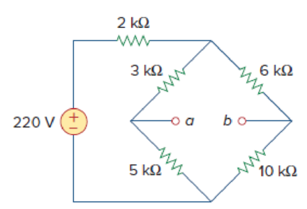
Figure 4.148
Find whether the bridge circuit of Figure 4.148 is balanced. Also find the value of the load resistor connected between the terminals a-b of the circuit and the maximum power absorbed by the load resistor.
Answer to Problem 92P
The bridge circuit is balanced when
Explanation of Solution
Given data:
Refer to Figure 4.148 in the textbook.
The voltage source is
Calculation:
For a bridge to be balanced, the voltage measured at terminals a-b should be zero.
The given circuit is modified as shown in Figure 1.
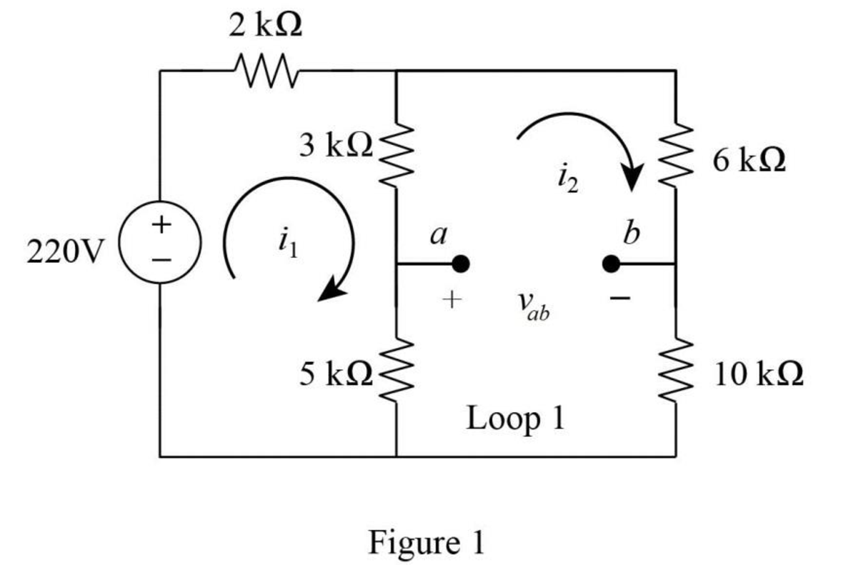
In Figure 1, apply Kirchhoff’s voltage law at loop
In Figure 1, apply Kirchhoff’s voltage law at loop
Substitute equation (2) in equation (1) as follows,
Simplify the equation as follows,
Substitute
In Figure 1, apply Kirchhoff’s voltage law at loop 1 as follows.
Substitute
As the voltage
In Figure 1, when the
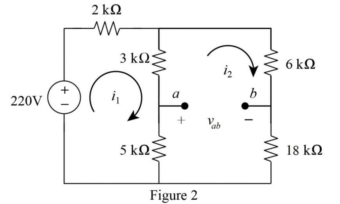
In Figure 2, apply Kirchhoff’s voltage law at loop
In Figure 2, apply Kirchhoff’s voltage law at loop
Substitute
Simplify the equation as follows,
Substitute
In Figure 2, the voltage
Substitute
Since the voltage
Refer to Figure (2).
In Figure (2), find the Thevenin resistance by turning off the
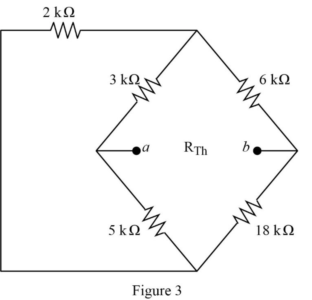
In Figure 3,
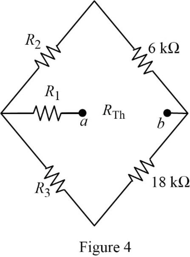
For the wye connection in Figure 4, the value of the resistor
For the wye connection in Figure 4, the value of the resistor
For the wye connection in Figure 4, the value of the resistor
Figure 4 is modified as shown in Figure 5.
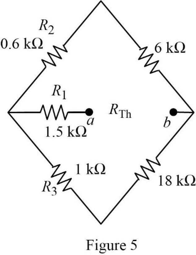
In Figure 5, the Thevenin resistance is,
Simplify the equation as follows,
For maximum power transfer,
The maximum power absorbed by the load resistor is,
Substitute
Conclusion:
Thus, the bridge circuit is balanced when
Want to see more full solutions like this?
Chapter 4 Solutions
EBK FUNDAMENTALS OF ELECTRIC CIRCUITS


- Find Va and Vb using nodal analysisarrow_forward2. Using the approximate method, hand sketch the Bode plot for the following transfer functions. a) H(s) = 10 b) H(s) (s+1) c) H(s): = 1 = +1 100 1000 (s+1) 10(s+1) d) H(s) = (s+100) (180+1)arrow_forwardQ4: Write VHDL code to implement the finite-state machine described by the state Diagram in Fig. 1. Fig. 1arrow_forward
- 1. Consider the following feedback system. Bode plot of G(s) is shown below. Phase (deg) Magnitude (dB) -50 -100 -150 -200 0 -90 -180 -270 101 System: sys Frequency (rad/s): 0.117 Magnitude (dB): -74 10° K G(s) Bode Diagram System: sys Frequency (rad/s): 36.8 Magnitude (dB): -99.7 System: sys Frequency (rad/s): 20 Magnitude (dB): -89.9 System: sys Frequency (rad/s): 20 Phase (deg): -143 System: sys Frequency (rad/s): 36.8 Phase (deg): -180 101 Frequency (rad/s) a) Determine the range of K for which the closed-loop system is stable. 102 10³ b) If we want the gain margin to be exactly 50 dB, what is value for K we should choose? c) If we want the phase margin to be exactly 37°, what is value of K we should choose? What will be the corresponding rise time (T) for step-input? d) If we want steady-state error of step input to be 0.6, what is value of K we should choose?arrow_forward: Write VHDL code to implement the finite-state machine/described by the state Diagram in Fig. 4. X=1 X=0 solo X=1 X=0 $1/1 X=0 X=1 X=1 52/2 $3/3 X=1 Fig. 4 X=1 X=1 56/6 $5/5 X=1 54/4 X=0 X-O X=O 5=0 57/7arrow_forwardQuestions: Q1: Verify that the average power generated equals the average power absorbed using the simulated values in Table 7-2. Q2: Verify that the reactive power generated equals the reactive power absorbed using the simulated values in Table 7-2. Q3: Why it is important to correct the power factor of a load? Q4: Find the ideal value of the capacitor theoretically that will result in unity power factor. Vs pp (V) VRIPP (V) VRLC PP (V) AT (μs) T (us) 8° pf Simulated 14 8.523 7.84 84.850 1000 29.88 0.866 Measured 14 8.523 7.854 82.94 1000 29.85 0.86733 Table 7-2 Power Calculations Pvs (mW) Qvs (mVAR) PRI (MW) Pay (mW) Qt (mVAR) Qc (mYAR) Simulated -12.93 -7.428 9.081 3.855 12.27 -4.84 Calculated -12.936 -7.434 9.083 3.856 12.32 -4.85 Part II: Power Factor Correction Table 7-3 Power Factor Correction AT (us) 0° pf Simulated 0 0 1 Measured 0 0 1arrow_forward
- Questions: Q1: Verify that the average power generated equals the average power absorbed using the simulated values in Table 7-2. Q2: Verify that the reactive power generated equals the reactive power absorbed using the simulated values in Table 7-2. Q3: Why it is important to correct the power factor of a load? Q4: Find the ideal value of the capacitor theoretically that will result in unity power factor. Vs pp (V) VRIPP (V) VRLC PP (V) AT (μs) T (us) 8° pf Simulated 14 8.523 7.84 84.850 1000 29.88 0.866 Measured 14 8.523 7.854 82.94 1000 29.85 0.86733 Table 7-2 Power Calculations Pvs (mW) Qvs (mVAR) PRI (MW) Pay (mW) Qt (mVAR) Qc (mYAR) Simulated -12.93 -7.428 9.081 3.855 12.27 -4.84 Calculated -12.936 -7.434 9.083 3.856 12.32 -4.85 Part II: Power Factor Correction Table 7-3 Power Factor Correction AT (us) 0° pf Simulated 0 0 1 Measured 0 0 1arrow_forwardelectric plants. Prepare the load schedulearrow_forwardelectric plants Draw the column diagram. Calculate the voltage drop. by hand writingarrow_forward
- electric plants. Draw the lighting, socket, telephone, TV, and doorbell installations on the given single-story project with an architectural plan by hand writingarrow_forwardA circularly polarized wave, traveling in the +z-direction, is received by an elliptically polarized antenna whose reception characteristics near the main lobe are given approx- imately by E„ = [2â, + jâ‚]ƒ(r. 8, 4) Find the polarization loss factor PLF (dimensionless and in dB) when the incident wave is (a) right-hand (CW) An elliptically polarized wave traveling in the negative z-direction is received by a circularly polarized antenna. The vector describing the polarization of the incident wave is given by Ei= 2ax + jay.Find the polarization loss factor PLF (dimensionless and in dB) when the wave that would be transmitted by the antenna is (a) right-hand CParrow_forwardjX(1)=j0.2p.u. jXa(2)=j0.15p.u. jxa(0)=0.15 p.u. V₁=1/0°p.u. V₂=1/0° p.u. 1 jXr(1) = j0.15 p.11. jXT(2) = j0.15 p.u. jXr(0) = j0.15 p.u. V3=1/0° p.u. А V4=1/0° p.u. 2 jX1(1)=j0.12 p.u. 3 jX2(1)=j0.15 p.u. 4 jX1(2)=0.12 p.11. JX1(0)=0.3 p.u. jX/2(2)=j0.15 p.11. X2(0)=/0.25 p.1. Figure 1. Circuit for Q3 b).arrow_forward
 Introductory Circuit Analysis (13th Edition)Electrical EngineeringISBN:9780133923605Author:Robert L. BoylestadPublisher:PEARSON
 Delmar's Standard Textbook Of ElectricityElectrical EngineeringISBN:9781337900348Author:Stephen L. HermanPublisher:Cengage Learning
 Programmable Logic ControllersElectrical EngineeringISBN:9780073373843Author:Frank D. PetruzellaPublisher:McGraw-Hill Education
 Fundamentals of Electric CircuitsElectrical EngineeringISBN:9780078028229Author:Charles K Alexander, Matthew SadikuPublisher:McGraw-Hill Education
 Electric Circuits. (11th Edition)Electrical EngineeringISBN:9780134746968Author:James W. Nilsson, Susan RiedelPublisher:PEARSON
 Engineering ElectromagneticsElectrical EngineeringISBN:9780078028151Author:Hayt, William H. (william Hart), Jr, BUCK, John A.Publisher:Mcgraw-hill Education,