Concept explainers
Videos
For the bridge circuit shown in Fig. 4.140, find the load RL for maximum power transfer and the maximum power absorbed by the load.
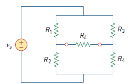
Figure 4.140
Find the maximum power transferred and maximum power absorbed by the load resistor
Answer to Problem 74P
The maximum power transferred and maximum power absorbed by the load resistor
Explanation of Solution
Given data:
Refer to Figure 4.140 in the textbook.
The voltage source is
Formula used:
Write the expression to find the power delivered to the resistor.
Here,
Calculation:
In the given circuit, find the Thevenin resistance by turning off the voltage source
The modified circuit is shown in Figure 1.
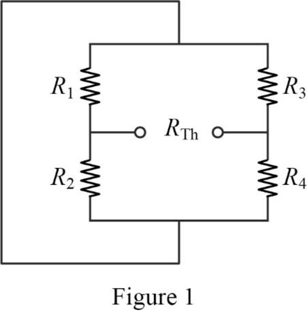
In Figure 1, the Thevenin resistance is,
Refer to Figure 4.139 in the textbook.
The given circuit is modified as shown in Figure 2 to find the Thevenin voltage.
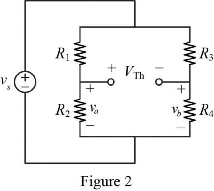
In Figure 2, the voltage
In Figure 2, the voltage
In Figure 2, apply Kirchhoff’s voltage law for the right bottom loop as follows.
Substitute
Substitute
Conclusion:
Thus, the maximum power transferred and maximum power absorbed by the load resistor
Want to see more full solutions like this?
Chapter 4 Solutions
EBK FUNDAMENTALS OF ELECTRIC CIRCUITS


- If C is the circle |z|=4 evaluate f f (z)dz for each of the following functions using residue. 1 f(z) = z(z²+6z+4)arrow_forwardIf C is the circle |z|=4 evaluate ff(z)dz for each of the following functions using residue. f(z) z(z²+6z+4)arrow_forwardDetermine X(w) for the given function shown in Figure (1) by applying the differentiation property of the Fourier Transform. 1 x(t) Figure (1) -2 I -1 1 2arrow_forward
- Please solve it by explaining the steps. I am trying to prepare for my exam tomorrow, so any tips and tricks to solve similar problems are highly appreciated. Plus, this is a past exam I am using to prepare.arrow_forwardPlease solve it by explaining the steps. I am trying to prepare for my exam tomorrow, so any tips and tricks to solve similar problems are highly appreciated. Plus, this is a past exam I am using to prepare.arrow_forwardPlease solve it by explaining the steps. I am trying to prepare for my exam tomorrow, so any tips and tricks to solve similar problems are highly appreciated. Plus, this is a past exam I am using to prepare.arrow_forward
- Please solve it by explaining the steps. I am trying to prepare for my exam tomorrow, so any tips and tricks to solve similar problems are highly appreciated. Plus, this is a past exam I am using to prepare.arrow_forwardPlease solve it by explaining the steps. I am trying to prepare for my exam tomorrow, so any tips and tricks to solve similar problems are highly appreciated. Plus, this is a past exam I am using to prepare.arrow_forwardPlease solve it by explaining the steps. I am trying to prepare for my exam tomorrow, so any tips and tricks to solve similar problems are highly appreciated. Plus, this is a past exam I am using to prepare.arrow_forward
- Please solve it by explaining the steps. I am trying to prepare for my exam tomorrow, so any tips and tricks to solve similar problems are highly appreciated. Plus, this is a past exam I am using to prepare.arrow_forwardPlease solve it by explaining the steps. I am trying to prepare for my exam tomorrow, so any tips and tricks to solve similar problems are highly appreciated. Plus, this is a past exam I am using to prepare.arrow_forwardPlease solve it by explaining the steps. I am trying to prepare for my exam tomorrow, so any tips and tricks to solve similar problems are highly appreciated. Plus, this is a past exam I am using to prepare.arrow_forward
 Introductory Circuit Analysis (13th Edition)Electrical EngineeringISBN:9780133923605Author:Robert L. BoylestadPublisher:PEARSON
 Delmar's Standard Textbook Of ElectricityElectrical EngineeringISBN:9781337900348Author:Stephen L. HermanPublisher:Cengage Learning
 Programmable Logic ControllersElectrical EngineeringISBN:9780073373843Author:Frank D. PetruzellaPublisher:McGraw-Hill Education
 Fundamentals of Electric CircuitsElectrical EngineeringISBN:9780078028229Author:Charles K Alexander, Matthew SadikuPublisher:McGraw-Hill Education
 Electric Circuits. (11th Edition)Electrical EngineeringISBN:9780134746968Author:James W. Nilsson, Susan RiedelPublisher:PEARSON
 Engineering ElectromagneticsElectrical EngineeringISBN:9780078028151Author:Hayt, William H. (william Hart), Jr, BUCK, John A.Publisher:Mcgraw-hill Education,