Concept explainers
Calculate the value of
Answer to Problem 91P
The value of
Explanation of Solution
Given data:
Refer Figure 3.127 in the textbook for the transistor circuit.
The common-emitter current gain
The base-emitter voltage
Formula used:
Write the expression for collector current in transistor.
Here,
Write the expression for emitter current of transistor.
Calculation:
The Thevenin resistance of the input circuit is the parallel combination of
The Thevenin voltage of the input circuit is the voltage across
Modify the Figure 3.127 with the incorporation of Thevenin equivalent circuit as shown in Figure 1.
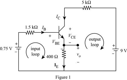
Apply Kirchhoff’s voltage law to input loop in Figure 1.
Substitute equation (2) in (3).
Substitute
Simplify the above equation as follows.
From Figure 1, write the expression for voltage
Substitute equation (2) in (4).
Substitute
Apply Kirchhoff’s voltage law to output loop in Figure 1.
Substitute equation (1) in (6).
Substitute
Conclusion:
Therefore, the value of
Want to see more full solutions like this?
Chapter 3 Solutions
Fundamentals of Electric Circuits


- Prelab Information 1. Laboratory Preliminary Discussion Second-order RC Circuit Analysis The second-order RC circuit shown in figure 1 below represents all voltages and impedances as functions of the complex variable, s. Note, of course, that the impedances associated with Rs, R₁, and R2 are constant independent of frequency, so the 's' notation is omitted. Again, one of the advantages of s-domain analysis is that we can apply all of the circuit analysis techniques learned for AC and DC circuits. To generate the s-domain expression for the output voltage, Vout(s) = Vc2(s), for the circuit shown in figure 1, we can apply voltage division in the s-domain as shown in equation 1 below. Equation 1 will be used in the prelab computations to find an expression for the output voltage, vc2(t), in the time domain. Note also that when we collect frequency response data for the circuit it will be operating at AC steady-state conditions for each frequency tested. Note that under AC steady-state…arrow_forwardDon't use ai to answer I will report you answerarrow_forwardThe power values of the loads in the circuit given in the figure are given below. Accordingly, which of the following is the RMS value of the Vs voltage amplitude? Load 1 (L1): the power factor is 1 and draws 13 kW of power,Load 2 (L2): draws 1 kVA at a forward power factor of 0.6,Load 3 (L3): draws 4 kW of average power and gives 3 kVAR of reactive power.arrow_forward
- The values of the elements in the circuit given in the figure are given below. Find the average power value on the R2 resistor. (Hint: First find the current of the R2 resistor with the loop current method. Four mutual inductance effect expressions should be added to each of the two loop equations.) Vs=238 voltsR1=13 ohmsR2=15 ohmsarrow_forwardDon't use ai to answer I will report you answerarrow_forwardA transformer bank is composed of three single-phase transformers of10kVA, 20kV/200V; copper losses are 100 W and core lossesthey are 50 W. The bank is connected in Delta on the high voltage side and in star on the sidethe low-voltage side. A. What are the values of voltages B.What are the values of currents C. losses in the core and losses in copper. D. nominal power of the transformer bank.Solve by one of the experts, not using artificial intelligencearrow_forward
- A 50 kVA, 13800/208 V transformer connected in Dy has an Rcc of 1% and aXcc of 7% per unit. A. What is the voltage regulation at full load and fp 0.8 in delay using the values of theimpedance (Ω).b. What is the voltage regulation under the same conditions using the system per unit Solve by one of the experts, not using artificial inteliggencearrow_forwardi need helppp pleasearrow_forwardsolve and show workarrow_forward
- 2) (15pts) In a PAM baseband digital communication system, an M-ary system has a channel bandwidth of 2 KHz. The channel introduces 10dB of losses and AWGN noise with a power spectral density of 1*10-6 W/Hz. The application requires a bit rate of 4.8 Kbps and BER of less than 10^-6. Estimate the require transmit power.arrow_forwardi need helppp pleasearrow_forward1) (2pts) If you know you have a bad clock (lots of jitter) and you are not bandwidth constrained, you should: (Circle the correct answer) a) Set the roll off factor to zero b) Set the roll off factor to ½ c) Set the roll off factor to one 2) (2pts) Short answer: Why do we use M-ary modulation? 3) (4 pts) Short answer: The application engineer comes to your desk and says that the error rate is too high and must be reduced for the application to function correctly. The system is battery operated. What do you tell them is the trade- off?arrow_forward
 Introductory Circuit Analysis (13th Edition)Electrical EngineeringISBN:9780133923605Author:Robert L. BoylestadPublisher:PEARSON
 Delmar's Standard Textbook Of ElectricityElectrical EngineeringISBN:9781337900348Author:Stephen L. HermanPublisher:Cengage Learning
 Programmable Logic ControllersElectrical EngineeringISBN:9780073373843Author:Frank D. PetruzellaPublisher:McGraw-Hill Education
 Fundamentals of Electric CircuitsElectrical EngineeringISBN:9780078028229Author:Charles K Alexander, Matthew SadikuPublisher:McGraw-Hill Education
 Electric Circuits. (11th Edition)Electrical EngineeringISBN:9780134746968Author:James W. Nilsson, Susan RiedelPublisher:PEARSON
 Engineering ElectromagneticsElectrical EngineeringISBN:9780078028151Author:Hayt, William H. (william Hart), Jr, BUCK, John A.Publisher:Mcgraw-hill Education,