Fundamentals of Electric Circuits
6th Edition
ISBN: 9780078028229
Author: Charles K Alexander, Matthew Sadiku
Publisher: McGraw-Hill Education
expand_more
expand_more
format_list_bulleted
Videos
Textbook Question
Chapter 3, Problem 78P
Solve Prob. 3.20 using PSpice or MultiSim.
3.20 For the circuit in Fig. 3.69, find v1, v2. and v3 using nodal analysis.
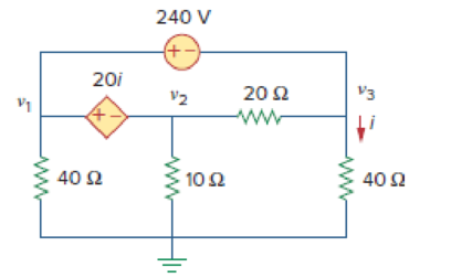
Figure 3.69
For Prob. 3.20.
Expert Solution & Answer
Want to see the full answer?
Check out a sample textbook solution
Students have asked these similar questions
Find Va and Vb using Nodal analysis
Calculate the nodal voltage in the circuit
Calculate the mesh currents, find Ia, Ib, Ic. Apply mesh analysis
Chapter 3 Solutions
Fundamentals of Electric Circuits
Ch. 3.2 - Figure 3.4 For Practice Prob. 3.1. Obtain the node...Ch. 3.2 - Figure 3.6 For Practice Prob. 3.2. Find the...Ch. 3.3 - Figure 3.11 For Practice Prob. 3.3. Find v and i...Ch. 3.3 - Figure 3.14 For Practice Prob. 3.4. Find v1, v2,...Ch. 3.4 - Practice Problem 3.5 Figure 3.19 For Practice...Ch. 3.4 - Practice Problem 3.6 Figure 3.21 For Practice...Ch. 3.5 - Practice Problem 3.7 Figure 3.25 For Practice...Ch. 3.6 - By inspection, obtain the node-voltage equations...Ch. 3.6 - By inspection, obtain the mesh-current equations...Ch. 3.8 - For the circuit in Fig. 3.33, use PSpice to find...
Ch. 3.8 - Use PSpice to determine currents i1, i2, and i3 in...Ch. 3.9 - For the transistor circuit in Fig. 3.42, let =...Ch. 3.9 - The transistor circuit in Fig. 3.45 has = 80 and...Ch. 3 - At node 1 in the circuit of Fig. 3.46, applying...Ch. 3 - Figure 3.46 For Review Questions 3.1 and 3.2 In...Ch. 3 - For the circuit in Fig. 3.47, v1 and v2 are...Ch. 3 - Figure 3.47 For Review Questions 3.3 and 3.4....Ch. 3 - The circuit i in the circuit of Fig. 3.48 is:...Ch. 3 - Figure 3.48 For Review Questions 3.5 and 3.6....Ch. 3 - In the circuit of Fig. 3.49, current i1 is: (a)4 A...Ch. 3 - Figure 3.49 For Review Questions 3.7 and 3.8....Ch. 3 - The PSpice part name for a current-controlled...Ch. 3 - Which of the following statements are not true of...Ch. 3 - Using Fig. 3.50, design a problem to help other...Ch. 3 - For the circuit in Fig. 3.51, obtain v1 and v2....Ch. 3 - Find the currents I1 through I4 and the voltage vo...Ch. 3 - Given the circuit in Fig. 3.53, calculate the...Ch. 3 - Obtain vo in the circuit of Fig. 3.54. Figure 3.54...Ch. 3 - Solve for V1 in the circuit of Fig. 3.55 using...Ch. 3 - Apply nodal analysis to solve for Vx in the...Ch. 3 - Using nodal analysis, find vo in the circuit of...Ch. 3 - Determine Ib in the circuit in Fig. 3.58 using...Ch. 3 - Prob. 10PCh. 3 - Find Vo and the power dissipated in all the...Ch. 3 - Using nodal analysis, determine Vo in the circuit...Ch. 3 - Calculate v1 and v2 in the circuit of Fig. 3.62...Ch. 3 - Using nodal analysis, find vo in the circuit of...Ch. 3 - Apply nodal analysis to find io and the power...Ch. 3 - Determine voltages v1 through v3 in the circuit of...Ch. 3 - Prob. 17PCh. 3 - Determine the node voltages in the circuit in Fig....Ch. 3 - Use nodal analysis to find v1, v2 and v3 in the...Ch. 3 - For the circuit in Fig. 3.69, find v1, v2, and v3...Ch. 3 - For the circuit in Fig. 3.70, find v1 and v2 using...Ch. 3 - Determine v1 and v2 in the circuit of Fig. 3.71....Ch. 3 - Use nodal analysis to find Vo in the circuit of...Ch. 3 - Use nodal analysis and MATLAB to find Vo in the...Ch. 3 - Use nodal analysis along with MATLAB to determine...Ch. 3 - Calculate the node voltages v1, v2, and v3 in the...Ch. 3 - Use nodal analysis to determine voltages v1, v2,...Ch. 3 - Use MATLAB to find the voltages at nodes a, b, c,...Ch. 3 - Use MATLAB to solve for the node voltages in the...Ch. 3 - Using nodal analysis, find vo and io in the...Ch. 3 - Find the node voltages for the circuit in Fig....Ch. 3 - Obtain the node voltages v1, v2, and v3 in the...Ch. 3 - Which of the circuits in Fig. 3.82 is planar? For...Ch. 3 - Determine which of the circuits in Fig. 3.83 is...Ch. 3 - Figure 3.54 For Prob. 3.5. Rework Prob. 3.5 using...Ch. 3 - Use mesh analysis to obtain ia, ib, and ic in the...Ch. 3 - Using nodal analysis, find vo in the circuit of...Ch. 3 - Apply mesh analysis to the circuit in Fig. 3.85...Ch. 3 - Using Fig. 3.50 from Prob. 3.1, design a problem...Ch. 3 - Prob. 40PCh. 3 - Apply mesh analysis to find i in Fig. 3.87. Figure...Ch. 3 - Using Fig. 3.88, design a problem to help students...Ch. 3 - Prob. 43PCh. 3 - Prob. 44PCh. 3 - Prob. 45PCh. 3 - Calculate the mesh currents i1 and i2 in Fig....Ch. 3 - Rework Prob. 3.19 using mesh analysis. Use nodal...Ch. 3 - Prob. 48PCh. 3 - Find vo and io in the circuit of Fig. 3.94. Figure...Ch. 3 - Prob. 50PCh. 3 - Apply mesh analysis to find vo in the circuit of...Ch. 3 - Use mesh analysis to find i1, i2 and i3 in the...Ch. 3 - Prob. 53PCh. 3 - Find the mesh currents i1, i2, and i3 in the...Ch. 3 - In the circuit of Fig. 3.100, solve for I1, I2,...Ch. 3 - Determine v1 and v2 in the circuit of Fig. 3.101....Ch. 3 - In the circuit of Fig. 3.102, find the values of...Ch. 3 - Find i1, i2, and i3 in the circuit of Fig. 3.103....Ch. 3 - Rework Prob. 3.30 using mesh analysis. Using nodal...Ch. 3 - Prob. 60PCh. 3 - Calculate the current gain iois in the circuit of...Ch. 3 - Find the mesh currents i1, i2, and i3 in the...Ch. 3 - Find vx and ix in the circuit shown in Fig. 3.107....Ch. 3 - Find vo and io in the circuit of Fig. 3.108.Ch. 3 - Use MATLAB to solve for the mesh currents in the...Ch. 3 - Write a set of mesh equations for the circuit in...Ch. 3 - Obtain the node-voltage equations for the circuit...Ch. 3 - Prob. 68PCh. 3 - For the circuit shown in Fig. 3.113, write the...Ch. 3 - Write the node-voltage equations by inspection and...Ch. 3 - Write the mesh-current equations for the circuit...Ch. 3 - Prob. 72PCh. 3 - Write the mesh-current equations for the circuit...Ch. 3 - By inspection, obtain the mesh-current equations...Ch. 3 - Use PSpice or MultiSim to solve Prob. 3.58....Ch. 3 - Use PSpice or MultiSim to solve Prob. 3.27....Ch. 3 - Solve for V1 and V2 in the circuit of Fig. 3.119...Ch. 3 - Solve Prob. 3.20 using PSpice or MultiSim. 3.20...Ch. 3 - Prob. 79PCh. 3 - Find the nodal voltages v1 through v4 in the...Ch. 3 - Use PSpice or MultiSim to solve the problem in...Ch. 3 - If the Schematics Netlist for a network is as...Ch. 3 - The following program is the Schematics Netlist of...Ch. 3 - Prob. 84PCh. 3 - An audio amplifier with a resistance of 9 ...Ch. 3 - Prob. 86PCh. 3 - For the circuit in Fig. 3.123, find the gain...Ch. 3 - Determine the gain vo/vs of the transistor...Ch. 3 - For the transistor circuit shown in Fig. 3.125,...Ch. 3 - Calculate vs for the transistor in Fig. 3.126...Ch. 3 - Prob. 91PCh. 3 - Prob. 92PCh. 3 - Rework Example 3.11 with hand calculation. In the...
Knowledge Booster


Learn more about
Need a deep-dive on the concept behind this application? Look no further. Learn more about this topic, electrical-engineering and related others by exploring similar questions and additional content below.Similar questions
- Find Va and Vb using Nodal analysisarrow_forward4. A battery operated sensor transmits to a receiver that is plugged in to a power outlet. The device is continuously operated. The battery is a 3.6 V coin-cell battery with a 245mAHr capacity. The application requires a bit rate of 36 Mbps and an error rate of less than 10^-3. The channel has a center frequency of 2.4 GHz, a bandwidth of 10 MHz and a noise power spectral density of 10^-14 W/Hz. The maximum distance is 36 meters and the losses in the channel attenuates the signal by 0.25 dB/meter. Your company has two families of chips that you can use. An M-ary ASK and an M-ary QAM chip. The have very different power requirements as shown in the table below. The total current for the system is the current required to achieve the desired Eb/No PLUS the current identified below: Hokies PSK Chip Set Operating Current NOT Including the required Eb/No for the application Hokies QAM Chip Set Operating Current NOT Including the required Eb/No for the application Chip ID M-ary Voltage (volts)…arrow_forwardUsing the 802.11a specifications given below, in Matlab (or similar tool) create the time domain signal for one OFDM symbol using QPSK modulation. See attached plot for the QPSK constellation. Your results should include the power measure in the time and frequency domain and comment on those results. BW 802.11a OFDM PHY Parameters 20 MHZ OBW Subcarrer Spacing Information Rate Modulation Coding Rate Total Subcarriers Data Subcarriers Pilot Subcarriers DC Subcarrier 16.6 MHZ 312.5 Khz (20MHz/64 Pt FFT) 6/9/12/18/24/36/48/54 Mbits/s BPSK, QPSK, 16QAM, 64QAM 1/2, 2/3, 3/4 52 (Freq Index -26 to +26) 48 4 (-21, -7, +7, +21) *Always BPSK Null (0 subcarrier) 52 subarriers -7 (48 Data, 4 Pilot (BPSK), 1 Null) -26 -21 0 7 21 +26 14 One Subcarrier 1 OFDM symbol 1 OFDM Burst -OBW 16.6 MHz BW 20 MHZ 1 constellation point = 52 subcarriers = one or more OFDM symbols 802.11a OFDM Physical Parameters Show signal at this point x bits do Serial Data d₁ S₁ Serial-to- Input Signal Parallel Converter IFFT…arrow_forward
- Find Vb and Va using Mesh analysisarrow_forward1. The communication channel bandwidth is 25 MHz centered at 1GHz and has a noise power spectral density of 10^-9 W/Hz. The channel loss between the transmitter and receiver is 25dB. The application requires a bit rate of 200Mbps and BER of less than 10^-4. Excluding Mary FSK, Determine the minimum transmit power required.arrow_forward2. An existing system uses noncoherent BASK. The application requires a BER of <10^-5. The current transmit power is 25 Watts. If the system changes to a coherent BPSK modulation scheme, what is the new transmit power required to deliver the same BER?arrow_forward
- 3. You are to design a 9-volt battery operated communication system that must last 3 years without replacing batteries. The communication channel bandwidth is 100 KHz centered at 5.8 GHz. The application requires a BER of <10^-5 and a data rate of 1 Mbps. The channel can be modeled as AWGN with a noise power spectral density of 10^-8 W/Hz. ((a) What modulation scheme would you use? B) what is the required capacity of the batteries? and (c) is the battery commercially available?arrow_forwardDesign a traffic light PIC microcontroller program with Green LED has 3 Sec Yellow LED has 0.5 Sec Red LED has 3 Sec RASAN4SSC20UT 8 RBOINT RB1 9 RB2 U1 PIC16F877A-I/PT 18 19 MCLRVPP RAOANO 20 RA1AN1 30 OSCICLKI 21 RAZAN2VREF-CVREF 31 OSC2CLKO RABAN3VREF+ 22 LED1 LED-3MM 〃 R1 330 RA4TOCKIC1OUT 23 7 VDD 28 VDD 6 VSS 29 VSS 24 LED2 LED-3MM R2 10 330 RB3PGM 11 + 14 RB4 38 RDOPSPO RB5 15 LED3 39 RD1PSP1 40 RD2PSP2 RB6PGC- RB7PGD 17 16 LED-3MM R3 330 41 RD3PSP3 2 RD4PSP4 RCOT1OSOTICKK 3 RDSPSPS RC1T10SICCP24 RD6PSP6 RC2CCP1 5 RD7PSP7 RC3SCKSCL RC4SDISDA 25 REORDANS RCSSDO 27 29 REIWRANG RC6TXCK- RE2CSAN7 RC7RXDT DAWWWW 32 35 36 37 42 43 44 1 12 NO 13 NC 33 NO 34 NCarrow_forward: +0 العنوان I need a detailed drawing with explanation しじ ined sove in peaper Anoting Q4// Draw and Evaluate √√√xy-²sin(y²)dydx PU+96er Lake Ge Q3// Find the volume of the region between the cylinder 2 = y² and the xy- plane that is bounded by the planes x = 1, x = 2, y = -2, and y = 2. T Marrow_forward
arrow_back_ios
SEE MORE QUESTIONS
arrow_forward_ios
Recommended textbooks for you
 Introductory Circuit Analysis (13th Edition)Electrical EngineeringISBN:9780133923605Author:Robert L. BoylestadPublisher:PEARSON
 Delmar's Standard Textbook Of ElectricityElectrical EngineeringISBN:9781337900348Author:Stephen L. HermanPublisher:Cengage Learning
 Programmable Logic ControllersElectrical EngineeringISBN:9780073373843Author:Frank D. PetruzellaPublisher:McGraw-Hill Education
 Fundamentals of Electric CircuitsElectrical EngineeringISBN:9780078028229Author:Charles K Alexander, Matthew SadikuPublisher:McGraw-Hill Education
 Electric Circuits. (11th Edition)Electrical EngineeringISBN:9780134746968Author:James W. Nilsson, Susan RiedelPublisher:PEARSON
 Engineering ElectromagneticsElectrical EngineeringISBN:9780078028151Author:Hayt, William H. (william Hart), Jr, BUCK, John A.Publisher:Mcgraw-hill Education,
Introductory Circuit Analysis (13th Edition)
Electrical Engineering
ISBN:9780133923605
Author:Robert L. Boylestad
Publisher:PEARSON
Delmar's Standard Textbook Of Electricity
Electrical Engineering
ISBN:9781337900348
Author:Stephen L. Herman
Publisher:Cengage Learning
Programmable Logic Controllers
Electrical Engineering
ISBN:9780073373843
Author:Frank D. Petruzella
Publisher:McGraw-Hill Education
Fundamentals of Electric Circuits
Electrical Engineering
ISBN:9780078028229
Author:Charles K Alexander, Matthew Sadiku
Publisher:McGraw-Hill Education
Electric Circuits. (11th Edition)
Electrical Engineering
ISBN:9780134746968
Author:James W. Nilsson, Susan Riedel
Publisher:PEARSON
Engineering Electromagnetics
Electrical Engineering
ISBN:9780078028151
Author:Hayt, William H. (william Hart), Jr, BUCK, John A.
Publisher:Mcgraw-hill Education,
Mesh Current Problems in Circuit Analysis - Electrical Circuits Crash Course - Beginners Electronics; Author: Math and Science;https://www.youtube.com/watch?v=DYg8B-ElK0s;License: Standard Youtube License