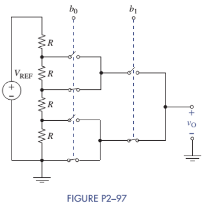
Programmable Voltage Divider Figure P2-97 shows a programmable voltage divider in which digital inputs b 0 and b 1 control complementary analog switches connecting a multitap voltage divider to the analog output vo. The switch positions in the figure apply when digital inputs are low. When inputs go high the switch positions reverse. Find the analog output voltage for ( b 1 , b 0 ) = ( 0 , 0 ) , ( 0 , 1 ) , ( 1 , 0 ) , and ( 1 , 1 ) when V REF = 12 V .
Programmable Voltage Divider Figure P2-97 shows a programmable voltage divider in which digital inputs b 0 and b 1 control complementary analog switches connecting a multitap voltage divider to the analog output vo. The switch positions in the figure apply when digital inputs are low. When inputs go high the switch positions reverse. Find the analog output voltage for ( b 1 , b 0 ) = ( 0 , 0 ) , ( 0 , 1 ) , ( 1 , 0 ) , and ( 1 , 1 ) when V REF = 12 V .
Solution Summary: The author describes the analog output voltage v_O for the given input values. The voltage across each resistor is equal to its resistance divided by the equivalent series resistance.
Figure P2-97 shows a programmable voltage divider in which digital inputs
b
0
and
b
1
control complementary analog switches connecting a multitap voltage divider to the analog output vo. The switch positions in the figure apply when digital inputs are low. When inputs go high the switch positions reverse. Find the analog output voltage for
(
b
1
,
b
0
)
=
(
0
,
0
)
,
(
0
,
1
)
,
(
1
,
0
)
,
and
(
1
,
1
)
when
V
REF
=
12
V
.
istics of diodes, bipolar junction transistors, and
plain the structure, operation,
1. The purpose of doping in semiconductor diodes is:
a) To control their electrical properties
b) To increase their physical size
c) To enhance their mechanical strength d) To improve their thermal stability
2. In electronics production, your team wants to manufacture a very cheap diode rectifier.
Which of the following rectifier configurations would you select?
a) Half-wave rectifier
c) Full-wave rectifier
b) Bridge rectifier
d) Controlled rectifier
3. The region that a Zener diode operates to provide voltage regulation is:
a) Saturation
c) Reverse bias
b) Breakdown
d) Forward bias
4. In NMOS transistors, the depth of the channel is primarily changed by:
a) VDS
b) lp
c) VGS
d) None of these
5. NMOS transistors have
than PMOS, resulting in better current conduction:
b) Long channel
a) High mobility
c) Low mobility
d) Short channel
6. You are working in electronic production, and your team is asked to…
8.46 The generator circuit shown in Fig. P8.46 (on page 494) isconnected to a distant load via a long coaxial transmission line.The overall circuit can be modeled as in Fig. P8.46(b), in whichthe transmission line is represented by an equivalent impedanceZline = (5+ j2) W.(a) Determine the power factor of voltage source Vs.(b) Specify the capacitance of a shunt capacitor C that wouldraise the power factor of the source to unity when connectedbetween terminals (a,b). The source frequency is 1.5 kHz.
7. MOSFET circuit
The MOSFET in the circuit below has V₁ = 1 V and kn = 4 mA/V².
a) Is the MOSFET operating in saturation or in the triode region?
b) Determine the drain current ID and Vout.
+ 5 V
5 k
Vout
Need a deep-dive on the concept behind this application? Look no further. Learn more about this topic, electrical-engineering and related others by exploring similar questions and additional content below.


 Introductory Circuit Analysis (13th Edition)Electrical EngineeringISBN:9780133923605Author:Robert L. BoylestadPublisher:PEARSON
 Delmar's Standard Textbook Of ElectricityElectrical EngineeringISBN:9781337900348Author:Stephen L. HermanPublisher:Cengage Learning
 Programmable Logic ControllersElectrical EngineeringISBN:9780073373843Author:Frank D. PetruzellaPublisher:McGraw-Hill Education
 Fundamentals of Electric CircuitsElectrical EngineeringISBN:9780078028229Author:Charles K Alexander, Matthew SadikuPublisher:McGraw-Hill Education
 Electric Circuits. (11th Edition)Electrical EngineeringISBN:9780134746968Author:James W. Nilsson, Susan RiedelPublisher:PEARSON
 Engineering ElectromagneticsElectrical EngineeringISBN:9780078028151Author:Hayt, William H. (william Hart), Jr, BUCK, John A.Publisher:Mcgraw-hill Education,