ANALYSIS+DESIGN OF LINEAR CIRCUITS(LL)
8th Edition
ISBN: 9781119235385
Author: Thomas
Publisher: WILEY
expand_more
expand_more
format_list_bulleted
Videos
Textbook Question
Chapter 2, Problem 2.93IP
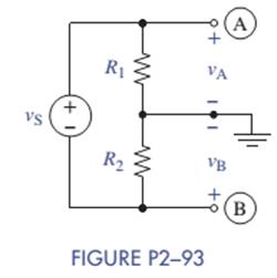
Center Tapped Voltage Divider
Figure P2-93 shows a voltage divider with the center tap connected to ground. Derive equations relating
Expert Solution & Answer
Want to see the full answer?
Check out a sample textbook solution
Students have asked these similar questions
(a) For the circuit shown in Figure Q3(a) (RFC and Cc are forbias)
(i)
(ii)
Draw the AC small signal equivalent circuit of the oscillator.
From this equivalent circuit derive an equation for fo and the gain condition for the
oscillations to start.
VDD
www
RG
eee
RFC
H
Cc
北
5
C₁
L
000
C₂
Vo
Please solve this question step by step handwritten solution and do not use chat gpt or any ai toolsfor part ii) you may need to use nodal analysis
12.1. Find the steady-state response vo (t) for the network.
00000-
1Ω
ww
12 cos(t) V
+
www
202
1 H
202
1 F
+
1Ω
νο
-
Chapter 2 Solutions
ANALYSIS+DESIGN OF LINEAR CIRCUITS(LL)
Ch. 2 - Prob. 2.1PCh. 2 - The voltage across a particular resistor is 8.60 V...Ch. 2 - You can choose to connect either a 4.7-k resistor...Ch. 2 - A model railroader wants to be able to...Ch. 2 - A 100-k resistor dissipates 50mW. Find the current...Ch. 2 - The conductance of a particular semiconductor...Ch. 2 - In Figure P2—7 the resistor dissipates 25 mW. Find...Ch. 2 - In Figure P2—8 find Rx and the power supplied by...Ch. 2 - A resistor found in the lab has three orange...Ch. 2 - The iv characteristic of a nonlinear resistor is...
Ch. 2 - A 100-k resistor has a power rating of 0.25 W....Ch. 2 - A certain type of film resistor is available with...Ch. 2 - Figure P2—13 shows the circuit symbol for a class...Ch. 2 - A thermistor is a temperature-sensing element...Ch. 2 - In Figure P2-15i2=6A and i3=2A. Find i1 and i4.Ch. 2 - In Figure P2-16 determine which elements are in...Ch. 2 - For the circuit in Figure P2—17: Identify the...Ch. 2 - In Figure P2-17 i2=30mA and i4=20mA. Find i1 and...Ch. 2 - For the circuit in Figure P2—19: Identify the...Ch. 2 - In Figure P2-19 v2=20V,v3=20V, and v4=6V. Find...Ch. 2 - In many circuits the ground is often the metal...Ch. 2 - The circuit in figure P2-22 is organized around...Ch. 2 - Are any of the elements in Figure P2-23 in series...Ch. 2 - Are any of the elements in Figure P2-24 in series...Ch. 2 - Use the passive sign convention to assign voltage...Ch. 2 - If a wire is connected between nodes B and C in...Ch. 2 - The KCL equations for a three-node circuit are as...Ch. 2 - For the circuit in Figure P2—28, write a complete...Ch. 2 - For the circuit in Figure P2—29, write a complete...Ch. 2 - Find vx and ix in Figure P2-30. Compare the...Ch. 2 - A modeler wants to light his model building using...Ch. 2 - Find vx and ix in Figure P2-32.Ch. 2 - In Figure P2-33: Assign a voltage and current...Ch. 2 - Find vO in the circuit of Figure P2-34.Ch. 2 - Find the power provided by the source in Figure...Ch. 2 - Figure P2-36 shows a subcircuit connected to the...Ch. 2 - In Figure P2-37 ix=0.33mA. Find the value of R.Ch. 2 - Figure P2—38 shows a resistor with one terminal...Ch. 2 - Find the equivalent resistant REQ in Figure P2-39.Ch. 2 - Find the equivalent R EQ in Figure P2-40.Ch. 2 - Find the equivalent resistance REQ in Figure...Ch. 2 - Equivalent resistance is defined at a particular...Ch. 2 - Find REQ in Figure P2—43 when the switch is open....Ch. 2 - Find REQ between nodes A and B for each of the...Ch. 2 - Show how the circuit in Figure P2—45 could be...Ch. 2 - In Figure P2-46 find the equivalent resistance...Ch. 2 - In Figure P2-47 find the equivalent resistance...Ch. 2 - Select a value of RL in Figure P2-48 so that...Ch. 2 - Using no more than four 1-k resistors, show how...Ch. 2 - Do a source transformation at terminals A and B...Ch. 2 - For each of the circuits in Figure P2-51, find the...Ch. 2 - In Figure P2-52, the iv characteristic of network...Ch. 2 - Select the value of Rx in Figure P2-53 so that...Ch. 2 - Two 10-k potentiometers (a variable resistor whose...Ch. 2 - Select the value of R in Figure P2-55 so that...Ch. 2 - What is the range of REQ in Figure P2-56?Ch. 2 - Find the equivalent resistance between terminals A...Ch. 2 - Use voltage division in Figure P2-58 to find...Ch. 2 - Use voltage division in Figure P2-59 to obtain an...Ch. 2 - Use current division in Figure P2-60 to find...Ch. 2 - Use current division in Figure P2-61 to find an...Ch. 2 - Find ix,iy, and iz in Figure P2-62.Ch. 2 - Find vO in the circuit of Figure P2-63.Ch. 2 - You wish to drive a 1-k load from your car battery...Ch. 2 - Find the range of values of vo in Figure P2-65.Ch. 2 - Use current division in the circuit of Figure...Ch. 2 - Figure P2-67 shows a voltage bridge circuit, that...Ch. 2 - A Ideally, a voltmeter has infinite internal...Ch. 2 - Select values for R1,R2, and R3 in Figure P2-69 so...Ch. 2 - Select a value of Rx in Figure P2-70 so that...Ch. 2 - Select a value of Rx in Figure P2-71 so that...Ch. 2 - Use circuit reduction to find vx and ix in Figure...Ch. 2 - Use circuit reduction to find vx,ix, and px in...Ch. 2 - Use circuit reduction to find vx and ix in Figure...Ch. 2 - Use circuit reduction to find vx,ix, and px in...Ch. 2 - Use circuit reduction to find vx and ix in Figure...Ch. 2 - Use source transformation to find ix in Figure...Ch. 2 - Select a value for Rx so that ix=0A in Figure...Ch. 2 - Use source transformations in Figure P2-79 to...Ch. 2 - The current through RL in figure P2-80 is 100mA....Ch. 2 - Select Rx so that 50 V is across it in Figure...Ch. 2 - The box in the circuit in Figure P2-82 is a...Ch. 2 - A circuit is found to have the following element...Ch. 2 - Consider the circuit of Figure P2-88. Use MATLAB...Ch. 2 - Nonlinear Device Characteristics The circuit in...Ch. 2 - Prob. 2.92IPCh. 2 - Center Tapped Voltage Divider Figure P2-93 shows a...Ch. 2 - Active Transducer Figure P2-95 shows an active...Ch. 2 - Programmable Voltage Divider Figure P2-97 shows a...Ch. 2 - Analog Voltmeter Design Figure P2-98(a) shows a...Ch. 2 - MATLAB Function for Parallel Equivalent Resistors...
Knowledge Booster


Learn more about
Need a deep-dive on the concept behind this application? Look no further. Learn more about this topic, electrical-engineering and related others by exploring similar questions and additional content below.Similar questions
- A Three-phase, 12 pole, Y-connected alternator has 108 slots and 14 conductors per slot. The windings are (5/6 th) pitched. The flux per pole is 57 mWb distributed sinusoidally over the pole. If the machine runs at 500 r.p.m., determine the following: (a) The frequency of the generated e.m.f., (b) The distribution factor, (c) The pitch factor, and (d) The phase and line values of the generated e.m.f.?arrow_forwardTwo 3-ph, 6.6 kV, Y-connected, alternators supply a load of 3000 kW at 0.8 p.f. lagging. The synchronou impedance per phase of machine A is (0.5+110) and that of machine B is (0.4 +J12) . The excitation of machine A adjusted so that it delivers 150 A. The load is shared equally between the machines. Determine the armature curre p.f., induced e.m.f., and load angle of each machine?arrow_forwardName the circuit below? The output voltage is initially zero and the pulse width is 200 μs. Find the Vout and draw the output waveform? +2.5 V V 247 -2.5 V C 0.01 F Ri W 10 ΚΩarrow_forward
- Please work outarrow_forwardFind Vfinal when Vs up and Vs V. Which LED will light in each case? Red or Green? Justify your answers. Fill the table below. Vs 8 ΚΩ Vos Χρι + 3 ΚΩ www 6 ΚΩ ww 4 ΚΩ Yo www Vo Vec-12 V Nol V final Vm w 3 ΚΩ 5 V 38 ΚΩ R= 1 kQ V -12 V Red LED Green LED Vs Vo Vfinal Which LED is ON? Varrow_forwardCircuits help please solve and explain. Question in images providedarrow_forward
- + V 6.2 A 1.2 A S R 4 Ω Find the source voltage Vs 0.8 Aarrow_forwardDetermine i(t) for t≥ 0 given that the circuit below had been in steady state for a long time prior to t = 0. Also, I₁ = 1 5 A, R₁ =22, R2 =10 Q2, R3 = 32, R4 =7 2, and L=0.15 H. Also fill the table. m L ww R2 t = 0 R₁ 29 R3 R4 Time 0 iL(t) 0 8arrow_forwardPlease help explain this problemarrow_forward
- + P = 16 W w w P = 8 W I R₁ R2 E = RT=322 1- Determine R1, R2, E ΙΩarrow_forward+ 30 V = - 20 V + R 2- Use KVL to find the voltage V - V + + 8 Varrow_forwardFind the Thévenin equivalent circuit for the portions of the networks in Figure external to the elements between points a and b. a R₁ 2002 I = 0.1 A 0° Xc : 32 Ω R2 = 6802 20 Ω фъarrow_forward
arrow_back_ios
SEE MORE QUESTIONS
arrow_forward_ios
Recommended textbooks for you
 Delmar's Standard Textbook Of ElectricityElectrical EngineeringISBN:9781337900348Author:Stephen L. HermanPublisher:Cengage Learning
Delmar's Standard Textbook Of Electricity
Electrical Engineering
ISBN:9781337900348
Author:Stephen L. Herman
Publisher:Cengage Learning
Lesson 2 - Source Transformations, Part 2 (Engineering Circuits); Author: Math and Science;https://www.youtube.com/watch?v=7gno74RhVGQ;License: Standard Youtube License