
Concept explainers
Videos
Consider the circuit in Figure P2.62. The output of a diode AND logic gate is connected to the input of a second diode AND logic gate. Assume
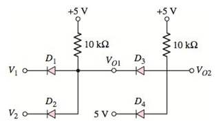
Figure P2.62
(a)
Values of output voltages
Answer to Problem 2.62P
The values of output voltages are
The values of output voltages are
The values of output voltages are
Explanation of Solution
Given:
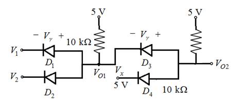
The given circuit is shown below.
Voltages given:
Calculation:
(i) Assume voltage
The entire circuit can be divided into two parts.
Now considering the first part,
On considering the connection of Diodes it is known that diodes are connected in reverse bias.
So, taking considerations from the first part, it is concluded that the output,
Hence, if the inputs of circuit are
Similarly, if the inputs of circuit are
Similarly, if the inputs of circuit are
Similarly, if the inputs of circuit are
Let’s make the truth table for
Table 1
| 0 0 5 5 | 0 5 0 | 0 0 0 5 |
On considering, the Boolean expression for
Now, taking considerations from the second part, as diodes are connected in reverse bias it is concluded that if any one of the inputs,
So the expression for the output voltage
Now for the given inputs
The diodes
Hence, from the expression for ideal diode output voltages are
(ii) Let’s assume voltage
The entire circuit can be divided into two parts.
Now considering the first part,
On considering the connection of Diodes it is known that diodes are connected in reverse bias.
So, taking considerations from the first part, it is concluded that the output,
Hence, if the inputs of circuit are
Similarly, if the inputs of circuit are
Similarly, if the inputs of circuit are
Similarly, if the inputs of circuit are
Let’s make the truth table for
Table 1
| 0 0 5 | 0 5 0 5 | 0 0 0 5 |
On considering, the Boolean expression for
Now, taking considerations from the second part, as diodes are connected in reverse bias it is concluded that if any one of the inputs,
So the expression for the output voltage
Now for the given inputs,
The diodes
Calculating the value of output voltage,
Calculating the value of output voltage,
Hence, output voltages are
(iii) Let’s assume voltage
The entire circuit can be divided into two parts.
Now considering the first part,
On considering the connection of Diodes it is known that diodes are connected in reverse bias.
So, taking considerations from the first part, it is concluded that the output,
Hence, if the inputs of circuit are
Similarly, if the inputs of circuit are
Similarly, if the inputs of circuit are
Similarly, if the inputs of circuit are
Let’s make the truth table for
Table 1
| 0 0 5 5 | 0 5 0 5 | 0 0 0 5 |
On considering, the Boolean expression for
Now, taking considerations from the second part, as diodes are connected in reverse bias it is concluded that if any one of the inputs,
So the expression for the output voltage
Now for the given inputs
The diodes
Calculating the value of output voltage,
Calculating the value of output voltage,
Hence, output voltages are
Therefore, in their LOW states the value of
(b)
Relative values of VO1 and VO2 in their “low” state
Answer to Problem 2.62P
Logic “0” signal degrades as it goes through additional logic gates.
Explanation of Solution
Given:
The given circuit is shown below.

Circuit diagram:

Logic “0” signal degrades as it goes through additional logic gates.
The diodes
Calculating the value of output voltage,
Calculating the value of output voltage,
Hence, output voltages are
Want to see more full solutions like this?
Chapter 2 Solutions
Microelectronics: Circuit Analysis and Design


- Find Io using Mesh analysisarrow_forwardFM station of 100 MHz carrier frequency modulated by a 20 kHz sinusoid with an amplitude of 10 volt, so that the peak frequency deviation is 25 kHz determine: 1) The BW of the FM signal. 2) The approximated BW if the modulating signal amplitude is increased to 50 volt. 3) The approximated BW if the modulating signal frequency is increased by 70%. 4) The amplitude of the modulating signal if the BW is 65 kHz.arrow_forwardAn FDM is used to multiplex two groups of signals using AM-SSB, the first group contains 25 speech signals, each has maximum frequency of 4 kHz, the second group contains 15 music signals, each has maximum frequency of 10 kHz. A guard bandwidth of 500 Hz is used bety each two signals and before the first one. 1. Find the BWmultiplexing 2. Find the BWtransmission if the multiplexing signal is modulated using AM-DSB-LC.arrow_forward
- An FM signal with 75 kHz deviation, has an input signal-to-noise ratio of 18 dB, with a modulating frequency of 15 kHz. 1) Find SNRO at demodulator o/p. 2) Find SNRO at demodulator o/p if AM is used with m=0.3. 3) Compare the performance in case 1) and 2).. Hint: for single tone AM-DSB-LC, SNR₁ = (2m²) (4)arrow_forwardFind Va and Vb using Nodal analysisarrow_forwardCalculate the nodal voltage in the circuitarrow_forward
- Calculate the mesh currents, find Ia, Ib, Ic. Apply mesh analysisarrow_forwardFind Va and Vb using Nodal analysisarrow_forward4. A battery operated sensor transmits to a receiver that is plugged in to a power outlet. The device is continuously operated. The battery is a 3.6 V coin-cell battery with a 245mAHr capacity. The application requires a bit rate of 36 Mbps and an error rate of less than 10^-3. The channel has a center frequency of 2.4 GHz, a bandwidth of 10 MHz and a noise power spectral density of 10^-14 W/Hz. The maximum distance is 36 meters and the losses in the channel attenuates the signal by 0.25 dB/meter. Your company has two families of chips that you can use. An M-ary ASK and an M-ary QAM chip. The have very different power requirements as shown in the table below. The total current for the system is the current required to achieve the desired Eb/No PLUS the current identified below: Hokies PSK Chip Set Operating Current NOT Including the required Eb/No for the application Hokies QAM Chip Set Operating Current NOT Including the required Eb/No for the application Chip ID M-ary Voltage (volts)…arrow_forward
- Using the 802.11a specifications given below, in Matlab (or similar tool) create the time domain signal for one OFDM symbol using QPSK modulation. See attached plot for the QPSK constellation. Your results should include the power measure in the time and frequency domain and comment on those results. BW 802.11a OFDM PHY Parameters 20 MHZ OBW Subcarrer Spacing Information Rate Modulation Coding Rate Total Subcarriers Data Subcarriers Pilot Subcarriers DC Subcarrier 16.6 MHZ 312.5 Khz (20MHz/64 Pt FFT) 6/9/12/18/24/36/48/54 Mbits/s BPSK, QPSK, 16QAM, 64QAM 1/2, 2/3, 3/4 52 (Freq Index -26 to +26) 48 4 (-21, -7, +7, +21) *Always BPSK Null (0 subcarrier) 52 subarriers -7 (48 Data, 4 Pilot (BPSK), 1 Null) -26 -21 0 7 21 +26 14 One Subcarrier 1 OFDM symbol 1 OFDM Burst -OBW 16.6 MHz BW 20 MHZ 1 constellation point = 52 subcarriers = one or more OFDM symbols 802.11a OFDM Physical Parameters Show signal at this point x bits do Serial Data d₁ S₁ Serial-to- Input Signal Parallel Converter IFFT…arrow_forwardFind Vb and Va using Mesh analysisarrow_forward1. The communication channel bandwidth is 25 MHz centered at 1GHz and has a noise power spectral density of 10^-9 W/Hz. The channel loss between the transmitter and receiver is 25dB. The application requires a bit rate of 200Mbps and BER of less than 10^-4. Excluding Mary FSK, Determine the minimum transmit power required.arrow_forward
