
Videos
(a)
Design a circuit which produces a transfer function of
(a)
Explanation of Solution
Given data:
The given transfer function is,
Calculation:
The transfer function of the circuit is,
The above transfer function has a zero at
The Figure 14.39 (b) in the textbook, that shows a cascade two stages of the circuit with a zero at
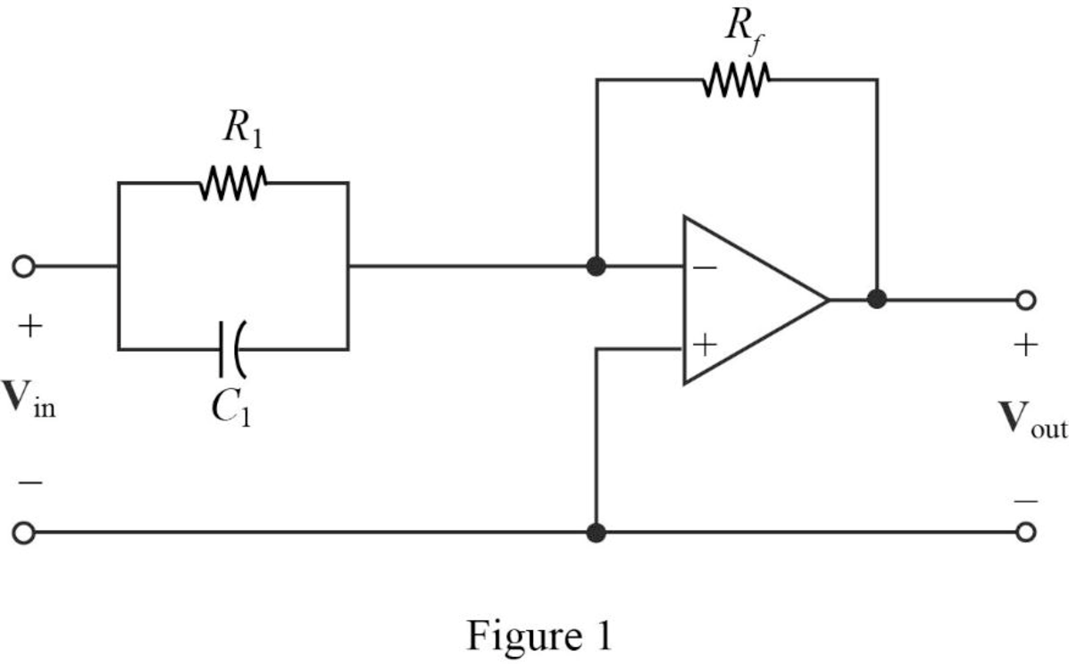
For a single zero,
Substitute
Consider the value of
Substitute
Transfer function:
The input impedance of the cascaded circuit in Figure 1 is,
Then, write the Formula for the transfer function for the cascaded two stage amplifier.
Substitute
Thus, the transfer function for
Substitute 1 for
Completing the design by letting
If the input will be inverted, add an inverting amplifier with gain of 1 to provide the transfer function as follows.
Thus, the final design of the circuit is,
Conclusion:
Thus, a circuit is designed which produces a transfer function of
(b)
Design a circuit which produces a transfer function of
(b)
Explanation of Solution
Given data:
The given transfer function is,
Calculation:
The transfer function of the circuit is,
The above transfer function has pole at
The Figure 14.39 (a) in the textbook, that shows a cascade two stages of the circuit with pole at
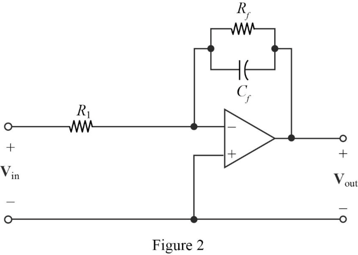
For pole
Substitute
Let arbitrarily consider
Substitute
Transfer function:
Find the feedback impedance of the cascaded circuit in Figure 2.
Write the formula for the transfer function of the cascaded circuit in Figure 2 as follows
Substitute
Therefore, consider the transfer function
Substitute 1 for
Completing the design by letting
If the input will be inverted, add an inverting amplifier with gain of 1 to provide the transfer function as follows.
Thus, the final design of the circuit is,
Conclusion:
Thus, a circuit is designed which produces a transfer function of
(c)
Design a circuit which produces a transfer function of
(c)
Explanation of Solution
Given data:
The given transfer function is,
Calculation:
The transfer function of the circuit is,
For the above transfer function, it has a zero at
Refer to Figure 1 in Part (a), that shows a cascade two stages of the circuit with a zero at
For a single zero,
Substitute
Let arbitrarily consider
Substitute
Consider the same circuit shown in Figure 1 and the transfer function as in a cascaded circuit,
Substitute 1 for
Completing the design by letting
Thus, the final design of the circuit is,
The given transfer function has a pole at
Refer to Figure 2 in Part (b), that shows a cascade two stages of the circuit with pole at
For pole
Substitute
Let arbitrarily consider
Substitute
The above equation becomes,
Consider the same circuit shown in Figure 2 and the transfer function as in a cascaded circuit,
Substitute 2 for
Completing the design by letting
Thus, the final design of the circuit is,
Therefore, the overall transfer function of the cascaded circuit is,
Substitute
Conclusion:
Thus, a circuit is designed which produces a transfer function of
Want to see more full solutions like this?
Chapter 14 Solutions
Loose Leaf for Engineering Circuit Analysis Format: Loose-leaf


- The capacitors in the circuit shown below have no energy stored in them and then switch “A” closes at time t=0. Find v(t) across the 6 uF capacitor for t≥0arrow_forwardConsider the circuit Below: A) Find and show the Thevenin equivalent with respect to terminals a,b B) Find and show the Norton equivalent with respect to terminals a,b C)Find the value of Ro and the maximum power delivered across it when its adjusted such that the power across it is the maximum possible when connected in this fashionarrow_forwardConsider the Circuit Below: A)Find Vo if Vin is 0.2 volts and the positive and negative power supply voltages are +15v and -15v respectively. B)What is the Maximum of Vin that will not hit saturation for this circuit?arrow_forward
- A shunt generator is rated at 125V, 25KW; armature resistance is 0.08 ohms, shunt field resistance is 25 ohms. What are: Armature voltage at rated load, armature power loss, shunt field power loss Total power generated in the armature?arrow_forwardA 12KW, 240V 1500RPM shunt generator has an armature resistance of .02 ohm and a shunt field resistance of 160 ohms. The stray power losses are 900W. Assuming a constant shunt field current, what (1) the efficiency at rated load and (2) the efficiency of the generator at half-rated load?arrow_forward4. Consider the three circuits shown in Figure. Determine each output voltage for (i) V₁ = 3 V and (ii) VI = -5 V. 40 ΚΩ www ww 20 ΚΩ 10 ΚΩ (a) 01 να гля 40 ΚΩ www www 20 ΚΩ 10 ΚΩ ww 10 ΚΩ www (b) www 48 ΚΩ ww -0% 6 kQ 15 ΚΩ (c) оооarrow_forward
- Find the mathematical expression for the points 1 and 2 for this pratical AM-DSB/SC modulatorarrow_forwardQuestion Two A generating station consisting of two generators, one of 20 MVA, 11 kV, 0.18 pu reactance with the unit transformer of 20 MVA, 11/132 kV, 0.08 pu reactance, another of 30 MVA, 11 kV, 0.18 pu reactance with the transformer of 30 MVA, 11/132 kV, 0.12 pu reactance, transmits power over double circuit 132-kV transmission line. Each line is having reactance of 120 ohms per phase. Determine the fault current supplied by the generators to a three-phase solid fault on the 132-kV bus-bar at the receiving end. Neglect pre-fault current and losses. Assume pre-fault generated voltages at rated value.arrow_forward4v+9v+8v=-3v+6v',-5v, where vi and vo are the input and output voltage, respectively.arrow_forward
- I decided to focus on the magnitude where I do the normalization on low and high pass and have the bandpass as dB(dB(decibel), with frequency cutoff, I manage to get accurate but have trouble controlling the frequency cutoff accurately and the bandbass isn't working properly. As such I need help.My Code: % Define frequency range for the plot f = logspace(1, 5, 500); % Frequency range from 10 Hz to 100 kHz w = 2 * pi * f; % Angular frequency % Parameters for the filters R = 1e3; % Resistance in ohms (1 kΩ) C = 1e-6; % Capacitance in farads (1 μF) L = 10e-3; % Inductance in henries (10 mH) % Transfer functions H_low = 1 ./ (1 + 1i * w * R * C); % Low-pass filter H_high = (1i * w * R * C) ./ (1 + 1i * w * R * C); % High-pass filter H_band = (1i * w * R * C) ./ (1 + 1i * w * L / R + 1i * w * R * C); % Band-pass filter % Cutoff frequency for RC filters (Low-pass and High-pass) f_cutoff_RC = 1 / (2 * pi * R * C); % Band-pass filter cutoff frequencies f_lower_cutoff = 1 / (2 * pi *…arrow_forwardPlease do NOT answer if you are going to use AI. Please give a proper solution.arrow_forwardP7.2 The capacitors in the circuit shown below have no energy stored in them and then switch "A" closes at time t=0. Switch "B" closes 2.5 milliseconds later. Find v(t) across the 6 μF capacitor for t≥ 0. 500 Ω B 4 µF 20 V 6 µF 7 Σ2 ΚΩ 25 mA + · μεarrow_forward
 Introductory Circuit Analysis (13th Edition)Electrical EngineeringISBN:9780133923605Author:Robert L. BoylestadPublisher:PEARSON
 Delmar's Standard Textbook Of ElectricityElectrical EngineeringISBN:9781337900348Author:Stephen L. HermanPublisher:Cengage Learning
 Programmable Logic ControllersElectrical EngineeringISBN:9780073373843Author:Frank D. PetruzellaPublisher:McGraw-Hill Education
 Fundamentals of Electric CircuitsElectrical EngineeringISBN:9780078028229Author:Charles K Alexander, Matthew SadikuPublisher:McGraw-Hill Education
 Electric Circuits. (11th Edition)Electrical EngineeringISBN:9780134746968Author:James W. Nilsson, Susan RiedelPublisher:PEARSON
 Engineering ElectromagneticsElectrical EngineeringISBN:9780078028151Author:Hayt, William H. (william Hart), Jr, BUCK, John A.Publisher:Mcgraw-hill Education,