Concept explainers
Videos
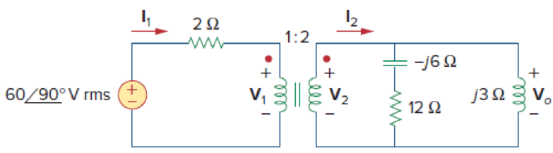
For the ideal transformer circuit of Fig. 13.122 below, find:
- (a) I1 and I2,
- (b) V1, V2, and Vo,
- (c) the complex power supplied by the source.
(a)
Calculate the currents
Answer to Problem 57P
The value of currents
Explanation of Solution
Given data:
Refer to Figure 13.122 in the textbook for the transformer circuit.
The value of n from the given figure is 2.
Calculation:
From Figure 13.122, calculate the load impedance
In Figure 13.122, reflect the load of
Substitute 2 for
Consider the expression for the impedance
Substitute
From Figure 1, write the expression for the current
Substitute
Write the expression for the current
Substitute
Conclusion:
Thus, the value of currents
(b)
Calculate the voltages
Answer to Problem 57P
The value of voltages
Explanation of Solution
Calculation:
Apply Kirchhoff's voltage law to the primary loop contains current
Substitute
Write the expression for the voltage
Substitute 2 for n and
Write the expression for the output voltage
Substitute
Conclusion:
Thus, The value of voltages
(c)
Calculate the complex power supplied by the source.
Answer to Problem 57P
The complex power supplied by the source is
Explanation of Solution
Calculation:
The conjugate of the current
Write the expression for the complex power supplied by the source.
Write the Matlab code to find the required complex power.
V=i*60;
I1_C=8.8753-i*24.3318;
S=V*I1_C
The output of the Matlab code is given as follows.
S = 1459.91 + 532.52i
From the Matlab output, the complex power is,
Conclusion:
Thus, the complex power supplied by the source is
Want to see more full solutions like this?
Chapter 13 Solutions
EBK FUNDAMENTALS OF ELECTRIC CIRCUITS


- Find Va and Vb using nodal analysisarrow_forward2. Using the approximate method, hand sketch the Bode plot for the following transfer functions. a) H(s) = 10 b) H(s) (s+1) c) H(s): = 1 = +1 100 1000 (s+1) 10(s+1) d) H(s) = (s+100) (180+1)arrow_forwardQ4: Write VHDL code to implement the finite-state machine described by the state Diagram in Fig. 1. Fig. 1arrow_forward
- 1. Consider the following feedback system. Bode plot of G(s) is shown below. Phase (deg) Magnitude (dB) -50 -100 -150 -200 0 -90 -180 -270 101 System: sys Frequency (rad/s): 0.117 Magnitude (dB): -74 10° K G(s) Bode Diagram System: sys Frequency (rad/s): 36.8 Magnitude (dB): -99.7 System: sys Frequency (rad/s): 20 Magnitude (dB): -89.9 System: sys Frequency (rad/s): 20 Phase (deg): -143 System: sys Frequency (rad/s): 36.8 Phase (deg): -180 101 Frequency (rad/s) a) Determine the range of K for which the closed-loop system is stable. 102 10³ b) If we want the gain margin to be exactly 50 dB, what is value for K we should choose? c) If we want the phase margin to be exactly 37°, what is value of K we should choose? What will be the corresponding rise time (T) for step-input? d) If we want steady-state error of step input to be 0.6, what is value of K we should choose?arrow_forward: Write VHDL code to implement the finite-state machine/described by the state Diagram in Fig. 4. X=1 X=0 solo X=1 X=0 $1/1 X=0 X=1 X=1 52/2 $3/3 X=1 Fig. 4 X=1 X=1 56/6 $5/5 X=1 54/4 X=0 X-O X=O 5=0 57/7arrow_forwardQuestions: Q1: Verify that the average power generated equals the average power absorbed using the simulated values in Table 7-2. Q2: Verify that the reactive power generated equals the reactive power absorbed using the simulated values in Table 7-2. Q3: Why it is important to correct the power factor of a load? Q4: Find the ideal value of the capacitor theoretically that will result in unity power factor. Vs pp (V) VRIPP (V) VRLC PP (V) AT (μs) T (us) 8° pf Simulated 14 8.523 7.84 84.850 1000 29.88 0.866 Measured 14 8.523 7.854 82.94 1000 29.85 0.86733 Table 7-2 Power Calculations Pvs (mW) Qvs (mVAR) PRI (MW) Pay (mW) Qt (mVAR) Qc (mYAR) Simulated -12.93 -7.428 9.081 3.855 12.27 -4.84 Calculated -12.936 -7.434 9.083 3.856 12.32 -4.85 Part II: Power Factor Correction Table 7-3 Power Factor Correction AT (us) 0° pf Simulated 0 0 1 Measured 0 0 1arrow_forward
- Questions: Q1: Verify that the average power generated equals the average power absorbed using the simulated values in Table 7-2. Q2: Verify that the reactive power generated equals the reactive power absorbed using the simulated values in Table 7-2. Q3: Why it is important to correct the power factor of a load? Q4: Find the ideal value of the capacitor theoretically that will result in unity power factor. Vs pp (V) VRIPP (V) VRLC PP (V) AT (μs) T (us) 8° pf Simulated 14 8.523 7.84 84.850 1000 29.88 0.866 Measured 14 8.523 7.854 82.94 1000 29.85 0.86733 Table 7-2 Power Calculations Pvs (mW) Qvs (mVAR) PRI (MW) Pay (mW) Qt (mVAR) Qc (mYAR) Simulated -12.93 -7.428 9.081 3.855 12.27 -4.84 Calculated -12.936 -7.434 9.083 3.856 12.32 -4.85 Part II: Power Factor Correction Table 7-3 Power Factor Correction AT (us) 0° pf Simulated 0 0 1 Measured 0 0 1arrow_forwardelectric plants. Prepare the load schedulearrow_forwardelectric plants Draw the column diagram. Calculate the voltage drop. by hand writingarrow_forward
- electric plants. Draw the lighting, socket, telephone, TV, and doorbell installations on the given single-story project with an architectural plan by hand writingarrow_forwardA circularly polarized wave, traveling in the +z-direction, is received by an elliptically polarized antenna whose reception characteristics near the main lobe are given approx- imately by E„ = [2â, + jâ‚]ƒ(r. 8, 4) Find the polarization loss factor PLF (dimensionless and in dB) when the incident wave is (a) right-hand (CW) An elliptically polarized wave traveling in the negative z-direction is received by a circularly polarized antenna. The vector describing the polarization of the incident wave is given by Ei= 2ax + jay.Find the polarization loss factor PLF (dimensionless and in dB) when the wave that would be transmitted by the antenna is (a) right-hand CParrow_forwardjX(1)=j0.2p.u. jXa(2)=j0.15p.u. jxa(0)=0.15 p.u. V₁=1/0°p.u. V₂=1/0° p.u. 1 jXr(1) = j0.15 p.11. jXT(2) = j0.15 p.u. jXr(0) = j0.15 p.u. V3=1/0° p.u. А V4=1/0° p.u. 2 jX1(1)=j0.12 p.u. 3 jX2(1)=j0.15 p.u. 4 jX1(2)=0.12 p.11. JX1(0)=0.3 p.u. jX/2(2)=j0.15 p.11. X2(0)=/0.25 p.1. Figure 1. Circuit for Q3 b).arrow_forward
 Introductory Circuit Analysis (13th Edition)Electrical EngineeringISBN:9780133923605Author:Robert L. BoylestadPublisher:PEARSON
 Delmar's Standard Textbook Of ElectricityElectrical EngineeringISBN:9781337900348Author:Stephen L. HermanPublisher:Cengage Learning
 Programmable Logic ControllersElectrical EngineeringISBN:9780073373843Author:Frank D. PetruzellaPublisher:McGraw-Hill Education
 Fundamentals of Electric CircuitsElectrical EngineeringISBN:9780078028229Author:Charles K Alexander, Matthew SadikuPublisher:McGraw-Hill Education
 Electric Circuits. (11th Edition)Electrical EngineeringISBN:9780134746968Author:James W. Nilsson, Susan RiedelPublisher:PEARSON
 Engineering ElectromagneticsElectrical EngineeringISBN:9780078028151Author:Hayt, William H. (william Hart), Jr, BUCK, John A.Publisher:Mcgraw-hill Education,