
Concept explainers
Videos
The overall small-signal voltage gain of the amplifier.
Answer to Problem 13.21P
The overall small-signal voltage gain of the amplifier is
Explanation of Solution
Given:
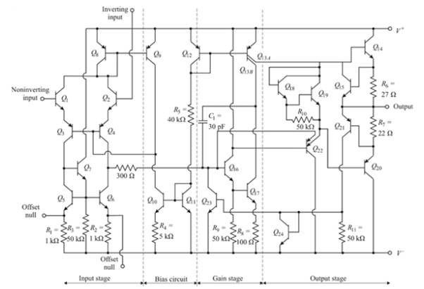
Consider the 741 op-amp having bias voltage ±5 V
Calculation:
The early voltage given as
The reference current is
Current
The bias currents in the input stage are,
The voltage at the collector of
The collector current in
Now, current
Assuming
The current in
The input resistance to the gain stage is found as
Therefore, the emitter resistor
Also,
Consequently, the resistor value
Now the resistance of the active load is determined as
And
Then,
Now the resistance
The small signal differential voltage is
The effective resistance of the active load is the resistance looking into the collector of
And the output resistance
The small signal voltage gain is
The overall gain is
Want to see more full solutions like this?
Chapter 13 Solutions
MICROELECT. CIRCUIT ANALYSIS&DESIGN (LL)


- A modulating signal f(t) is bandlimited to 5 kHz is sampled at a rate of 15000 samples/sec. The samples are quantized into 128 levels. Calculate the transmission bandwidth if the following modulation types are used for signal transmission: 4- ASK 5- 8-PSK 6- FSK with Af = 25 kHzarrow_forwardA modulating signal f(t) is bandlimited to 5 kHz is sampled at a rate of 15000 samples/sec. The samples are quantized into 128 levels. Calculate the transmission bandwidth if the following modulation types are used for signal transmission: 4- ASK 5- 8-PSK 6- FSK with Af = 25 kHzarrow_forwardDon't use ai to answer I will report you answerarrow_forward
- jan G(f) f Sketch the spectrum of g(t), which has a maximum frequency of 5 kHz, if it is sampled at the following sampling frequencies: 7 kHz, 10 kHz and 15 kHz. Indicate if and how the signal can be recovered at each sampling frequency.arrow_forwardDon't use ai to answer i will report your answerarrow_forwardA single tone is modulated using FM transmitter. The SNR, at the input of the demodulator 20 dB. If the maximum frequency of the modulating signal is 4 kHz, and the maximum equency deviation is 12 kHz, find the SNR, and the bandwidth (using Carson rule) at the ollowing conditions: . For the given values of fm and Af. !. If the amplitude of the modulating signal is increased by 80%. 3. If the amplitude of the modulating signal is decreased by 50%, and frequency of modulating signal is increased by 50%.arrow_forward
- The circuit shown below on the left has the following parameters: V₁ = 5 V. R₁ = 40, R₂ = 40, α = 0.1. This circuit can be replaced by an equivalent circuit shown below on the right such that the voltage and current received by an arbitrary load resistor RL, are identical when connected to either circuits. Determine the value of the resistor R (in ) in the equivalent circuit. R₁ Rx R2 R₁ Vx R₁ Vi απ. barrow_forward1. Consider the following a unity feedback control system. R(s) + E(s) 500(s+2)(s+5)(s+6) s(s+8)(s+10)(s+12) -Y(s) Find the followings: a) Type of the system b) Static position error constant Kp, Static velocity error constant Ry and Static acceleration error constant Ka c) Find the steady-state error of the system for (i) step input 1(t), (ii) ramp input t 1(t), (iii) parabolic input t² 1(t). 2. Repeat the above problem for the following system. R(s) + E(s) 500(s + 2)(s + 5) (s+8)(s+ 10)(s+12) Y(s) 3. Repeat the above problem for the following system. R(s) + E(s) 500(s+2)(s+4)(s+5)(s+6)(s+7) s²(s+8)(s+10)(s+12) Y(s)arrow_forward4. Consider a unity (negative) feedback control system whose open-loop transfer function is given by the following. 2 G(s) = s³ (s + 2) Find the steady-state error of the system for each of the following inputs. = a) u(t) (t²+8t+5) 1(t) b) u(t) = 3t³ 1(t) c) u(t) (t+5t² - 1) 1(t) =arrow_forward
- 1 2. For the following closed-loop system, G(s) = and H(s) = ½ (s+4)(s+6) a. Please draw the root locus by hand and mark the root locus with arrows. Calculate the origin and angle for asymptotes. b. Use Matlab to draw the root locus to verify your sketch. Input R(s) Output C(s) KG(s) H(s)arrow_forward5. Consider following feedback system. R(s) + 100 S+4 +1 Find the steady-state error for (i) step input and (ii) ramp input.arrow_forward6. Find (i) settling time (Ts), (ii) rise time (Tr), (iii) peak time (Tp), and (iv) percent overshoot (% OS) for each of the following systems whose transfer functions are given by: a) H(s) = 5 s²+12s+20 5 b) H(s) = s²+6s+25 c) H(s) = (s+2) (s²+12s+20) (s²+4s+13) Use dominant pole approximation if needed.arrow_forward
 Introductory Circuit Analysis (13th Edition)Electrical EngineeringISBN:9780133923605Author:Robert L. BoylestadPublisher:PEARSON
 Delmar's Standard Textbook Of ElectricityElectrical EngineeringISBN:9781337900348Author:Stephen L. HermanPublisher:Cengage Learning
 Programmable Logic ControllersElectrical EngineeringISBN:9780073373843Author:Frank D. PetruzellaPublisher:McGraw-Hill Education
 Fundamentals of Electric CircuitsElectrical EngineeringISBN:9780078028229Author:Charles K Alexander, Matthew SadikuPublisher:McGraw-Hill Education
 Electric Circuits. (11th Edition)Electrical EngineeringISBN:9780134746968Author:James W. Nilsson, Susan RiedelPublisher:PEARSON
 Engineering ElectromagneticsElectrical EngineeringISBN:9780078028151Author:Hayt, William H. (william Hart), Jr, BUCK, John A.Publisher:Mcgraw-hill Education,