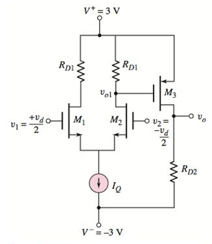
Consider the simple MOS op−amp circuit shown in Figure P13.1. The biascurrent is

Figure P13.1
Want to see the full answer?
Check out a sample textbook solution
Chapter 13 Solutions
MICROELECT. CIRCUIT ANALYSIS&DESIGN (LL)
- Not use ai pleasearrow_forward49. For the circuit below, what is the best connection of the capacitor to filte voltage? ბი DO A O BO wwwww wwwww M m H E LOADarrow_forward5.25. Determine the corner frequency resulting from Cin in Fig. 5.47(d). For simplicity, assume C₁ is a short circuit. TVDD C₁ M2 RF Vin H w - Vout Cin M₁arrow_forward
- In the below circuit, find out the value of equivalent Thevenin's voltage and Thevenin's resistance at the terminal. 2000 0.25 A 400 2 800 2 0.1 Aarrow_forwardQ1: For the circuit shown in Figure-1, (a) Calculate the equivalent resistance of the circuit, RAB at the terminals A and B. [10] (b) When 50V dc source is switched at terminals A-B, solve for the voltage V₁ at the location shown. [10] 50V www 12Ω 10Ω 5Ω www www A + B 200 Figure-1 www 10Ω ww 25Ω 100arrow_forwarda. Write a PLC ladder diagram that allows the teacher to teach AND, OR, and XOR logic gates through using three PLC's digital input points and only one digital output point.arrow_forward
- rately by PRACTICE 4.2 For the circuit of Fig. 4.5, compute the voltage across each curren source. 202 ww 3A 30 ww 4Ω S 50 www Reference node FIGURE 4.5 Ans: V3A =5.235 V; 7A = 11.47 V. 7 Aarrow_forwardQ2) a) design and show me your steps to convert the following signal from continuous form to digital form: s(t)=3sin(3πt) -1 373 Colesarrow_forwardA sequence is defined by the relationship r[n] = [h[m]h[n+m]=hn*h-n where h[n] is a minimum-phase sequence and r[n]= 4 4 (u[n]+ 12" [n-1] 3 (a) Find R(z) and sketch the pole-zero diagram. (b) Determine the minimum-phase sequence h[n] to within a scale factor of ±1. Also, determine the z-transform H(z) of h[n].arrow_forward
- usıng j-k and D flipflop design a counter that counts 0,2,1 again as shown below ın the tablearrow_forwardfind the minterms of the followıng boolean expressıon desıgn F's cırcuit using one of the approciate decoders given below and a NOR gateF(A,B,C,D)=(A+'BC)(B 'C+'A 'D + CD)arrow_forward64) answer just two from three the following terms: A) Design ADC using the successive method if the Vmax=(3) volt, Vmin=(-2) volt, demonstrate the designing system for vin-1.2 volt. Successive Approximation ADC Input Voltage-1.1 V -4-3.5-3 -2.5 -2 -1.5 +1 -0.5 0 0.5 1 1.5 2 2.5 3 3.5 1 T -8 -7 -6 -5 -3 +2 -1 0 1 2 3 4 5 6 7 X=1??? 1st guess: -0.25 V (too high) X=11?? 2nd guess: -2.25 V (too low) 3rd guess: -1.25 V (too low) X=1110 X=111? 4th guess: -0.75 V (too high) Make successive guesses and use a comparator to tell whether your guess is too high or too low. Each guess determines one bit of the answer and cuts the number of remaining possibilities in half.arrow_forward
 Introductory Circuit Analysis (13th Edition)Electrical EngineeringISBN:9780133923605Author:Robert L. BoylestadPublisher:PEARSON
 Delmar's Standard Textbook Of ElectricityElectrical EngineeringISBN:9781337900348Author:Stephen L. HermanPublisher:Cengage Learning
 Programmable Logic ControllersElectrical EngineeringISBN:9780073373843Author:Frank D. PetruzellaPublisher:McGraw-Hill Education
 Fundamentals of Electric CircuitsElectrical EngineeringISBN:9780078028229Author:Charles K Alexander, Matthew SadikuPublisher:McGraw-Hill Education
 Electric Circuits. (11th Edition)Electrical EngineeringISBN:9780134746968Author:James W. Nilsson, Susan RiedelPublisher:PEARSON
 Engineering ElectromagneticsElectrical EngineeringISBN:9780078028151Author:Hayt, William H. (william Hart), Jr, BUCK, John A.Publisher:Mcgraw-hill Education,


