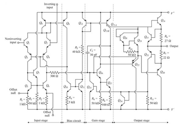
The overall small-signal voltage gain of the amplifier.
Answer to Problem 13.20P
The overall small-signal voltage gain of the amplifier is
Explanation of Solution
Given:
Consider the 741 op-amp having bias voltage ±5 V

Calculation:
The reference current is.
Current
The bias currents in the input stage are,
The voltage at the collector of
The collector current in
Now, current
Assuming
The current in
The input resistance to the gain stage is found as
Therefore, the emitter resistor
Also
Consequently, the resistor value
Now the resistance of the active load is determined as
And
Then
Now the resistance
The small signal differential voltage is
The effective resistance of the active load is the resistance looking into the collector of
The small signal voltage gain is
The overall gain is
Want to see more full solutions like this?
Chapter 13 Solutions
Microelectronics: Circuit Analysis and Design
- 7.48 Determine the Thevenin equivalent of the circuit inFig. P7.48 at terminals (a,b), given thatVs(t) = 12cos 2500t V,Is(t) = 0.5cos(2500t −30◦) A.arrow_forward1. In the following closed-loop system, a PD controller of the form K(s + 5) is used. Design the gain K such that the system achieves an overshoot of 16%. Calculate the settling time and peak time for the PD controlled system. Compensator R(s) + E(s) Plant 1 C(s) K(s+Zc) (s+1)(s+2)(s+5)arrow_forwardFind Voarrow_forward
- 3. Use MATLAB to generate the Nyquist plot for the following system. Then, apply the Nyquist stability criterion to determine the range of K values that ensure the stability of the closed-loop system. R(s)+ K C(s) (s+2) 1 (s + 4)(s+6)arrow_forward4. Please find the stability margins from the following Bode diagrams. Bode Diagram Phase (deg) Magnitude (dB) 50 -100 -90 -135 -180 -270 10" 10° Frequency (rad/sec) 10'arrow_forward2. Please use asymptotes to draw the Bode diagrams of the following transfer function. Please label the axes to show the cut-off frequencies and key values on vertical axes and label each asymptote with its slope. G(s) s+10 s(s²+10s+100)arrow_forward
 Introductory Circuit Analysis (13th Edition)Electrical EngineeringISBN:9780133923605Author:Robert L. BoylestadPublisher:PEARSON
 Delmar's Standard Textbook Of ElectricityElectrical EngineeringISBN:9781337900348Author:Stephen L. HermanPublisher:Cengage Learning
 Programmable Logic ControllersElectrical EngineeringISBN:9780073373843Author:Frank D. PetruzellaPublisher:McGraw-Hill Education
 Fundamentals of Electric CircuitsElectrical EngineeringISBN:9780078028229Author:Charles K Alexander, Matthew SadikuPublisher:McGraw-Hill Education
 Electric Circuits. (11th Edition)Electrical EngineeringISBN:9780134746968Author:James W. Nilsson, Susan RiedelPublisher:PEARSON
 Engineering ElectromagneticsElectrical EngineeringISBN:9780078028151Author:Hayt, William H. (william Hart), Jr, BUCK, John A.Publisher:Mcgraw-hill Education,


