Concept explainers
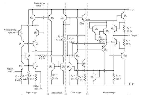
The output resistance of the 741 op-amp if
Answer to Problem 13.24P
The output resistance is
Explanation of Solution
Given:
Consider the 741 op-amp having bias voltage ±5 V

Calculation:
The resistance at
And the output resistance is defined as
Now for solving equation (1) we have
Assuming series resistance of
Where,
And
Where,
The collector current in
The reference current is.
The collector current in
Assuming
And from equation (7),
Now, the current
And the current
Now the resistance
The resistance
Now from the equation (5),
Now from equation (4),
From the equation (3),
Now from the equation (1),
Now from the equation (2),
Want to see more full solutions like this?
Chapter 13 Solutions
Microelectronics: Circuit Analysis and Design
- How can I design a socket for a trolley headlight? What parameters should I measure? The only thing I have is the headlight itself, and I don’t have any information about its power, current, or voltage rating. The power source is 120 V, and my goal is simply to get the headlight to turn on.I’m not sure where to start or what to measure. Any recommendations would be greatly appreciated!arrow_forwardFigure 2 3) *** The circuit of Figure 3 is designed with W/L = 20/0.18, λ= 0, and ID = 0.25 mA. (Optional- 20 points) a) Compute the required gate bias voltage. b) With such a gate voltage, how much can W/L be increased while M1 remains in saturation? What is the maximum voltage gain that can be achieved as W/L increases? VDD = 1.8 V RD 2k - Vout Vin M₁ Figure 3arrow_forward1) Rs = 4kQ, R₁ = 850 kQ, R₂ = 350 kQ, and R₁ = 4 kQ. The transistor parameters are VTP = -12 V, K'p = 40 µA / V², W/L = 80, and λ = 0.05 V-1. (50 Points) a) Determine IDQ and VSDQ. b) Find the small signal voltage gain. (Av) c) Determine the small signal circuit transconductance gain. (Ag = io/vi) d) Find the small signal output resistance. VDD = 10 V 2'; www www Figure 1 Ссarrow_forward
 Introductory Circuit Analysis (13th Edition)Electrical EngineeringISBN:9780133923605Author:Robert L. BoylestadPublisher:PEARSON
 Delmar's Standard Textbook Of ElectricityElectrical EngineeringISBN:9781337900348Author:Stephen L. HermanPublisher:Cengage Learning
 Programmable Logic ControllersElectrical EngineeringISBN:9780073373843Author:Frank D. PetruzellaPublisher:McGraw-Hill Education
 Fundamentals of Electric CircuitsElectrical EngineeringISBN:9780078028229Author:Charles K Alexander, Matthew SadikuPublisher:McGraw-Hill Education
 Electric Circuits. (11th Edition)Electrical EngineeringISBN:9780134746968Author:James W. Nilsson, Susan RiedelPublisher:PEARSON
 Engineering ElectromagneticsElectrical EngineeringISBN:9780078028151Author:Hayt, William H. (william Hart), Jr, BUCK, John A.Publisher:Mcgraw-hill Education,


