EBK FUNDAMENTALS OF ELECTRIC CIRCUITS
6th Edition
ISBN: 8220102801448
Author: Alexander
Publisher: YUZU
expand_more
expand_more
format_list_bulleted
Concept explainers
Videos
Textbook Question
Chapter 5, Problem 64P
For the op amp circuit shown in Fig. 5.91, find vo/vs.
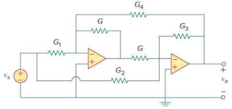
Figure 5.91
For Prob. 5.64.
Expert Solution & Answer
Want to see the full answer?
Check out a sample textbook solution
Students have asked these similar questions
Not use ai please
NEED HANDWRITTEN SOLUTION DO NOT USE AI OR CHATGPT
2) Determine the voltage gain of the follower depicted in Fig. 2. Assume Is= 7 × 10-16.
B = 100, VA = 5 V. Also assume the capacitors are very large. (40 points)
Chapter 5 Solutions
EBK FUNDAMENTALS OF ELECTRIC CIRCUITS
Ch. 5.2 - If the same 741 op amp in Example 5.1 is used in...Ch. 5.3 - Repeat Example 5.1 using the ideal op amp model....Ch. 5.4 - Practice Problem 5.3 Figure 5.13 For Practice...Ch. 5.4 - Two kinds of current-to-voltage converters (also...Ch. 5.5 - Calculate vo in the circuit of Fig. 5.20. Answer:...Ch. 5.6 - Practice Problem 5.6 Find vo and io in the op amp...Ch. 5.7 - Design a difference amplifier with gain 7.5....Ch. 5.7 - Obtain io in the instrumentation amplifier circuit...Ch. 5.8 - Practice Problem 5.9 Figure 5.30 For Practice...Ch. 5.8 - If v1 = 5 V and v2 = 5 V, find vo in the op amp...
Ch. 5.9 - Rework Practice Prob. 5.1 using PSpice. If the...Ch. 5.10 - A three-bit DAC is shown in Fig. 5.37. (a)...Ch. 5.10 - Determine the value of the external gain-setting...Ch. 5 - The two input terminals of an op amp are labeled...Ch. 5 - For an ideal op amp, which of the following...Ch. 5 - For the circuit in Fig. 5.40, voltage vo is: (a)6...Ch. 5 - For the circuit in Fig. 5.40, current ix is:...Ch. 5 - If vs = 0 in the circuit of Fig. 5.41, current io...Ch. 5 - If vs = 8 mV in the circuit of Fig. 5.41, the...Ch. 5 - Refer to Fig. 5.41. If vs = 8 mV, voltage va is:...Ch. 5 - The power absorbed by the 4-k resistor in Fig....Ch. 5 - Which of these amplifiers is used in a...Ch. 5 - Difference amplifiers are used in (please check...Ch. 5 - The equivalent model of a certain op amp is shown...Ch. 5 - The open-loop gain of an op amp is 50,000....Ch. 5 - Determine the voltage input to the inverting...Ch. 5 - The output voltage of an op amp is 4 V when the...Ch. 5 - For the op amp circuit of Fig. 5.44, the op amp...Ch. 5 - Using the same parameters for the 741 op amp in...Ch. 5 - 5.7 The op amp in Fig. 5.46 has Ri = 100 k, Ro =...Ch. 5 - Obtain vo for each of the op amp circuits in Fig....Ch. 5 - Determine vo for each of the op amp circuits in...Ch. 5 - Prob. 10PCh. 5 - Using Fig. 5.50, design a problem to help other...Ch. 5 - Calculate the voltage ratio vo/vs for the op amp...Ch. 5 - Find vo and io in the circuit of Fig. 5.52. Figure...Ch. 5 - Determine the output voltage vo in the circuit of...Ch. 5 - (a)Determine the ratio vo/is in the op amp circuit...Ch. 5 - Using Fig. 5.55, design a problem to help students...Ch. 5 - Prob. 17PCh. 5 - For the circuit shown in Figure 5.57, solve for...Ch. 5 - Determine io in the circuit of Fig. 5.58. Figure...Ch. 5 - In the circuit of Fig. 5.59, calculate vo of vs =...Ch. 5 - Calculate vo in the op amp circuit of Fig. 5.60....Ch. 5 - Design an inverting amplifier with a gain of 15.Ch. 5 - For the op amp circuit in Fig. 5.61, find the...Ch. 5 - In the circuit shown in Fig. 5.62, find k in the...Ch. 5 - Calculate vo in the op amp circuit of Fig. 5.63....Ch. 5 - Using Fig. 5.64, design a problem to help other...Ch. 5 - Find vo in the op amp circuit of Fig. 5.65. Figure...Ch. 5 - Prob. 28PCh. 5 - Determine the voltage gain vo/vi of the op amp...Ch. 5 - In the circuit shown in Fig. 5.68, find ix and the...Ch. 5 - For the circuit in Fig. 5.69, find ix. Figure 5.69...Ch. 5 - Calculate ix and vo in the circuit of Fig. 5.70....Ch. 5 - Refer to the op amp circuit in Fig. 5.71....Ch. 5 - Given the op amp circuit shown in Fig. 5.72,...Ch. 5 - Design a noninverting amplifier with a gain of...Ch. 5 - For the circuit shown in Fig. 5.73, find the...Ch. 5 - Determine the output of the summing amplifier in...Ch. 5 - Using Fig. 5.75, design a problem to help other...Ch. 5 - For the op amp circuit in Fig. 5.76, determine the...Ch. 5 - Referring to the circuit shown in Fig. 5.77,...Ch. 5 - An averaging amplifier is a summer that provides...Ch. 5 - The feedback resistor of a three-input averaging...Ch. 5 - The feedback resistor of a five-input averaging...Ch. 5 - Show that the output voltage vo of the circuit in...Ch. 5 - Design an op amp circuit to perform the following...Ch. 5 - Using only two op amps, design a circuit to solve...Ch. 5 - The circuit in Fig. 5.79 is for a difference...Ch. 5 - The circuit in Fig. 5.80 is a differential...Ch. 5 - Design a difference amplifier to have a gain of 4...Ch. 5 - Design a circuit to amplify the difference between...Ch. 5 - Using two op amps, design a subtractor.Ch. 5 - Design an op amp circuit such that vo = 4v1 + 6v2 ...Ch. 5 - The ordinary difference amplifier for fixed-gain...Ch. 5 - Determine the voltage transfer ratio vovs in the...Ch. 5 - In a certain electronic device, a three-stage...Ch. 5 - Using Fig. 5.83, design a problem to help other...Ch. 5 - Find vo in the op amp circuit of Fig. 5.84.Ch. 5 - Calculate io in the op amp circuit of Fig. 5.85....Ch. 5 - In the op amp circuit of Fig. 5.86, determine the...Ch. 5 - Calculate vo/vi in the op amp circuit of Fig....Ch. 5 - Determine vo in the circuit of Fig. 5.88. Figure...Ch. 5 - Obtain the closed-loop voltage gain vo/vi of the...Ch. 5 - Determine the gain vovi of the circuit in Fig....Ch. 5 - For the op amp circuit shown in Fig. 5.91, find...Ch. 5 - Find vo in the op amp circuit of Fig. 5.92.Ch. 5 - For the circuit in Fig. 5.93, find vo.Ch. 5 - Obtain the output vo in the circuit of Fig. 5.94....Ch. 5 - Find vo in the circuit of Fig. 5.95, assuming that...Ch. 5 - Find vo in the circuit of Fig. 5.95, assuming that...Ch. 5 - Determine vo in the op amp circuit of Fig. 5.96.Ch. 5 - Determine vo in the op amp circuit of Fig. 5.97.Ch. 5 - Find the load voltage vL in the circuit of Fig....Ch. 5 - Determine the load voltage vL in the circuit of...Ch. 5 - Find io in the op amp circuit of Fig. 5.100....Ch. 5 - Rework Example 5.11 using the nonideal op amp...Ch. 5 - Solve Prob. 5.19 using PSpice or MultiSim and op...Ch. 5 - Solve Prob. 5.48 using PSpice or MultiSim and op...Ch. 5 - Use PSpice or MultiSim to obtain vo in the circuit...Ch. 5 - Determine vo in the op amp circuit of Fig. 5.102,...Ch. 5 - Use PSpice or MultiSim to solve Prob. 5.70....Ch. 5 - Use PSpice or MultiSim to verify the results in...Ch. 5 - Prob. 82PCh. 5 - Design a six-bit digital-to-analog converter. (a)...Ch. 5 - A four-bit R-2R ladder DAC is presented in Fig....Ch. 5 - In the op amp circuit of Fig. 5.104, find the...Ch. 5 - Design a voltage controlled ideal current source...Ch. 5 - Figure 5.105 displays a two-op-amp instrumentation...Ch. 5 - Figure 5.106 shows an instrumentation amplifier...Ch. 5 - Design a circuit that provides a relationship...Ch. 5 - The op amp circuit in Fig. 5.107 is a current...Ch. 5 - A noninverting current amplifier is portrayed in...Ch. 5 - Refer to the bridge amplifier shown in Fig. 5.109....Ch. 5 - A voltage-to-current converter is shown in Fig....
Knowledge Booster


Learn more about
Need a deep-dive on the concept behind this application? Look no further. Learn more about this topic, electrical-engineering and related others by exploring similar questions and additional content below.Similar questions
- Calculate the voltage gain and I/O impedance of circuits shown in Fig. 1. Assume (60 points- each section 20 points) J Vina кат Vb J Vina кат VCC VCC VCC Vino - Vout - Vout Rs w Q2 Q2 (c) (b) Q2 = (a) - Voutarrow_forwardNot use ai please letarrow_forwardUse PSpice to create the circuit and show the circuit along with simulation results. Also please explicitly answer the question (i.e. have the answer make sense and not in parts where there is no final answer.)arrow_forward
- Problem 5 Plot the impulse response of the system shown below. Hint: This is done graphically with 4 convolutions. x[n] D y[n]< D D D D D D D D D D Darrow_forwardUse PSpice to create the circuit. Also please explicitly answer whether the load line intersects the -0.7 line at the computed point.arrow_forwardIn class, we wrote on the blackboard a byte addressable memory where each element was 2 nibbles: For example: Main memory A Address Offset Data Data Data Data Data Data Data Data Data Data Data Data Data Data Data Data 0 1 2 3 4 5 6 0 Ox10 0x00 0x02 0x2B Ox4F 0x00 0x00 0x00 0x11 0x12 0x20 0x10 0x10 0x00 OxFF Ox3E DxDD 0x00 0x00 0x00 0x00 0x00 0x00 0x00 7 0x1C 0x00 8 9 A 0x00 0x00 0x01 0x00 0x00 0x01 0x00 0x00 0x01 B с D E 0x00 0x05 0x04 0x03 0x02 0x00 Ox3D 0x00 0x1C Ox2F 0x00 Ox1F OxFF 0x03 0x02 F What is the contents of address 0x1C in main memory A for a 32 bit machine using Big Endian format? What is the contents of address 0x1C in main memory A for a 16 bit machine using Little Endian format? What is the contents of the indirect address at 0x04 in main memory A for a Big Endian 32 bit machine ((0x4))? What is the contents of 4(0x10) in main memory A for a 16 bit Little Endian machine? What is the contents of the address 16(0xC) for a 64 bit Little Endian machine?arrow_forward
- Problem 4 Consider the system shown below where h₁[n] = {2,1,2} and h₂[n] = (n+1) u[n] (− means subtraction). h₂[n] x [n]- h₁[n] бел-27- h₂[n] y[n] (a) Determine the impulse response of the system and plot it for n = -3,...,6. (b) Determine graphically the response of the system to the following input. x[n] 2 4 5arrow_forwardNot use ai pleasearrow_forwardDesign a self-biased JFET circuit (Fig. 6) assuming VGS(0) = -1.3 and ipss= 20 mA. We require a VGS = -0.7. Assume a supply voltage of 15 volts. Draw the load line for this circuit using Fig. 4b once you have selected the appropriate values for the components. Does the load line intersect the VGS = -0.7 volt line at the computed in point? RD. RG Rs 12 20nA GS = -1.3 VGS 10nA Fig. 6. Circuit for Examples 2 &3. 50 100 150 200 □ ID(J1) UDS Fig. 4b. The IV characteristics of an n-channel JFET (J113). The plots are for VGs increments of 0.05 volts. VGS(0) -1.3. The yellow and blue load lines are for examples 2 &3, respectively.arrow_forward
- Find the operating point and the load line of a voltage-divider JFET biasing circuit using the following parameters: VGS(0) = -1.3 and Vcc = 15 volts. Assume ipss = 20 mA, RG₁ = RG2 = 10 kn, RD = 300, and Rs = 1 kn. Use Fig. 4b for the IV characteristic of the JFET. 20nA GS=-1.3 GS 10nA- 50 100 150 200 ID(J1) UDS Fig. 4b. The IV characteristics of an n-channel JFET (J113). The plots are for VGs increments of 0.05 volts. VGS(0) -1.3. The yellow and blue load lines are for examples 2 &3, respectively.arrow_forwardDesign the JFET circuit for the largest in swing. Use the self-bias circuit shown in Fig. 6. Assume that VGS (0) = -1.3 and Vcc = 15 volts. Furthermore, assume that ipss = 20 mA. Using Fig. 4b, draw the load line and identify the Q point. Explain why this will allow the largest swing. Use ip = ipss (1- VGS VGS(0) to show what happens to i, and vps when you have a swing of 0.2 volts in vcs form its operating point (that is, change vas by ±0.2 volts and compute the corresponding iD and VDs). RD RG Rs 0 20nA GS=-1.3 VGS 12 10nA -0- Fig. 6. Circuit for Examples 2 &3. BA-C 50 100 150 200 □ ID(J1) UDS Fig. 4b. The IV characteristics of an n-channel JFET (J113). The plots are for VGs increments of 0.05 volts. VGS(0) -1.3. The yellow and blue load lines are for examples 2 &3, respectively.arrow_forwardplease do the correct VI chrastaristics curve on excel. I am not sure if mine is correctarrow_forward
arrow_back_ios
SEE MORE QUESTIONS
arrow_forward_ios
Recommended textbooks for you
 Introductory Circuit Analysis (13th Edition)Electrical EngineeringISBN:9780133923605Author:Robert L. BoylestadPublisher:PEARSON
 Delmar's Standard Textbook Of ElectricityElectrical EngineeringISBN:9781337900348Author:Stephen L. HermanPublisher:Cengage Learning
 Programmable Logic ControllersElectrical EngineeringISBN:9780073373843Author:Frank D. PetruzellaPublisher:McGraw-Hill Education
 Fundamentals of Electric CircuitsElectrical EngineeringISBN:9780078028229Author:Charles K Alexander, Matthew SadikuPublisher:McGraw-Hill Education
 Electric Circuits. (11th Edition)Electrical EngineeringISBN:9780134746968Author:James W. Nilsson, Susan RiedelPublisher:PEARSON
 Engineering ElectromagneticsElectrical EngineeringISBN:9780078028151Author:Hayt, William H. (william Hart), Jr, BUCK, John A.Publisher:Mcgraw-hill Education,
Introductory Circuit Analysis (13th Edition)
Electrical Engineering
ISBN:9780133923605
Author:Robert L. Boylestad
Publisher:PEARSON
Delmar's Standard Textbook Of Electricity
Electrical Engineering
ISBN:9781337900348
Author:Stephen L. Herman
Publisher:Cengage Learning
Programmable Logic Controllers
Electrical Engineering
ISBN:9780073373843
Author:Frank D. Petruzella
Publisher:McGraw-Hill Education
Fundamentals of Electric Circuits
Electrical Engineering
ISBN:9780078028229
Author:Charles K Alexander, Matthew Sadiku
Publisher:McGraw-Hill Education
Electric Circuits. (11th Edition)
Electrical Engineering
ISBN:9780134746968
Author:James W. Nilsson, Susan Riedel
Publisher:PEARSON
Engineering Electromagnetics
Electrical Engineering
ISBN:9780078028151
Author:Hayt, William H. (william Hart), Jr, BUCK, John A.
Publisher:Mcgraw-hill Education,
Electrical Engineering: Ch 5: Operational Amp (2 of 28) Inverting Amplifier-Basic Operation; Author: Michel van Biezen;https://www.youtube.com/watch?v=x2xxOKOTwM4;License: Standard YouTube License, CC-BY