ANALYSIS+DESIGN OF LINEAR CIRCUITS(LL)
8th Edition
ISBN: 9781119235385
Author: Thomas
Publisher: WILEY
expand_more
expand_more
format_list_bulleted
Concept explainers
Videos
Textbook Question
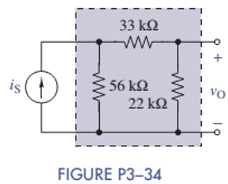
Chapter 3, Problem 3.34P
Find the proportionality constant
Expert Solution & Answer
Want to see the full answer?
Check out a sample textbook solution
Students have asked these similar questions
Consider the following 4×1 multiplexer with inputs:
w0=2, w1=1, w2=x2' and w3=0
And with switches:
S1 x1 and S0=x0
What is the multiplexer output f as a function of x2, x1
and x0?
I need help adding a capacitor and a Zener diode to my circuit. I’m looking for a simple sketch or diagram showing how to connect them. i want diagram with final circuit after adding the zener diad and capacitor. don't do calclution or anything. thanks
Question 3 AC Motor Drives [15]Calculate the instantaneous currents delivered by the inverter if the direct axiscurrent required at a particular instant is 8.66A and the quadrature current is5A. Derive all equations for the three currents.
Chapter 3 Solutions
ANALYSIS+DESIGN OF LINEAR CIRCUITS(LL)
Ch. 3 - Formulate node-voltage equations for the circuit...Ch. 3 - (a) Formulate node-voltage equations for the...Ch. 3 - (a) Formulate node-voltage equations for the...Ch. 3 - Formulate node-voltage equations for the circuit...Ch. 3 - (a) Formulate node-voltage equations for the...Ch. 3 - Choose a ground wisely and formulate node-voltage...Ch. 3 - The following are a set of node-voltage equations;...Ch. 3 - Choose a ground wisely and formulate node-voltage...Ch. 3 - Formulate node-voltage equations for the circuit...Ch. 3 - Formulate node-voltage equations for the circuit...
Ch. 3 - (a) Formulate mesh-current equations for the...Ch. 3 - (a) Formulate mesh-current equations for the...Ch. 3 - (a) Formulate mesh-current equations for the...Ch. 3 - Prob. 3.16PCh. 3 - Formulate mesh-current equations for the circuit...Ch. 3 - For the circuit of figure P3-19 solve for iA,iB,...Ch. 3 - Formulate mesh-current equations for the circuit...Ch. 3 - The circuit in Figure P3-21 seems to require two...Ch. 3 - Formulate mesh-current equations for the circuit...Ch. 3 - Use simple engineering intuition to find the input...Ch. 3 - In Figure P3-24 all of the resistors are 1k and...Ch. 3 - Use Figure P3-24 and MATLAB to solve the following...Ch. 3 - Formulate mesh-current equations for the circuit...Ch. 3 - Find vO for the block diagram shown in figure...Ch. 3 - Design a voltage-divider circuit that will realize...Ch. 3 - Design a current-divider circuit that will realize...Ch. 3 - Using a single resistor, design a circuit that...Ch. 3 - Find the proportionality constant K=vO/vS for the...Ch. 3 - Find the proportionality constant K=iO/vS for the...Ch. 3 - Find the proportionality constant K=vO/iS for the...Ch. 3 - Find the proportionality constant K=iO/iS for the...Ch. 3 - Find the proportionality constant K=vO/vS for the...Ch. 3 - Use the unit output method to find K and vO in...Ch. 3 - Use the unit output method to find K and vO in...Ch. 3 - Use the unit output method to find K in Figure...Ch. 3 - Use the superposition principle to find vO in...Ch. 3 - Use the superposition principle to find vO in...Ch. 3 - Use the superposition principle to find vO in...Ch. 3 - (a) Use the superposition principle to find vO in...Ch. 3 - A linear circuit containing two sources drives a...Ch. 3 - A block diagram of a linear circuit is shown in...Ch. 3 - A certain linear circuit has four input voltages...Ch. 3 - When the current source is turned off in the...Ch. 3 - For the circuit in Figure P3—51, find the Thévenin...Ch. 3 - For the circuit in Figure P3—52, find the Thévenin...Ch. 3 - For the circuit of Figure P3—53, find the Thévenin...Ch. 3 - Find the Thévenin or Norton equivalent circuit...Ch. 3 - Find the Thévenin or Norton equivalent circuit...Ch. 3 - Find the Thévenin equivalent circuit seen by RL in...Ch. 3 - Find the Norton equivalent seen by RL in Figure...Ch. 3 - You need to determine the Thévenin equivalent...Ch. 3 - Find the Thévenin equivalent seen by RL in figure...Ch. 3 - The purpose of this problem is to use Thévenin...Ch. 3 - The circuit in Figure P3-62 was solved earlier...Ch. 3 - Assume that Figure P3-63 represents a model of the...Ch. 3 - The iv characteristic of the active circuit...Ch. 3 - You have successfully completed the first course...Ch. 3 - The Thévenin equivalent parameters of a practical...Ch. 3 - Use a sequence of source transformations to find...Ch. 3 - The circuit in Figure P3-68 provides power to a...Ch. 3 - A nonlinear resistor is connected across a...Ch. 3 - Prob. 3.71PCh. 3 - Find the Norton equivalent seen by RL in Figure...Ch. 3 - Find the Thévenin equivalent seen by RL in Figure...Ch. 3 - Find the Thévenin equivalent seen by RL in Figure...Ch. 3 - For the circuit of Figure P3-75, find the value of...Ch. 3 - For the circuit of Figure P3-76, find the value of...Ch. 3 - The resistance R in Figure P3-77 is adjusted until...Ch. 3 - When a 5-k resistor is connected across a...Ch. 3 - Find the value of R in the circuit of Figure P3-79...Ch. 3 - For the circuit of Figure P3-80, find the value of...Ch. 3 - A 1-k load needs 10 mA to operate correctly....Ch. 3 - A practical source delivers 25 mA to a load. The...Ch. 3 - A 10-V source is shown in Figure P3-83 that is...Ch. 3 - (a)Select RL and design an interface circuit for...Ch. 3 - The source in Figure P3-85 has a 100-mA output...Ch. 3 - Figure P3-86 shows an interface circuit connecting...Ch. 3 - Prob. 3.87PCh. 3 - In this problem, you will design two interface...Ch. 3 - Two teams are competing to design the interface...Ch. 3 - The bridge-T attenuation pad shown in FigureP3-90...Ch. 3 - Design two interface circuits in Figure P3-91 so...Ch. 3 - Design the interface circuit in Figure P3-91 so...Ch. 3 - Design the interface circuit in Figure P3-93 so...Ch. 3 - It is claimed that both interface circuits in...Ch. 3 - Audio Speaker Resistance-Matching Network A...Ch. 3 - Interface Circuit Design Using no more than three...Ch. 3 - Battery Design A satellite requires a battery with...Ch. 3 - Design Interface Competition The output of a...Ch. 3 - Prob. 3.106IP
Knowledge Booster


Learn more about
Need a deep-dive on the concept behind this application? Look no further. Learn more about this topic, electrical-engineering and related others by exploring similar questions and additional content below.Similar questions
- A certain signal f(t) has the following PSD (assume 12 load): Sp (w) = new + 8(w) - 1.5) + (w + 1.5)] (a) What is the mean power in the bandwidth w≤2 rad/see? (b) What is the mean power in the bandwidth -1.9 to 0.99 rad/sec? Paress(w) dw 2ㅈ -arrow_forward(75 Marks) JA signal (t) is bond 7)(t)(t) and f(t), are band-limited to 1.2 kHz each. These signals are to be limited to 9.6 kHz, and three other signals transmitted by means of time-division multiplexing. Set up scheme for accomplishing this multiplexing requirement, with each signal sampled at its Nyquist rate. What must be the speed of the commutator (the output but ram-k bit/sec)? the minimum band width? (25 Marks)arrow_forwardDraw the digital modulation outputs, ASK Amplitude Shift Keying) FSK (Frequency Shift Keying) and PSK (Phase Shift Keying). For baseband and carriet frequency as shown 101 wwwwwwwwwwww 010 BASESAND basband CARRIER Carralarrow_forward
- please show full working. I've included the solutionarrow_forwardcan you please show working and steps. The answer is 8kohms.arrow_forwardPSD A certain signal f(t) has the following PSD (assume 12 load): | Sƒ(w) = π[e¯\w\ + 8(w − 2) + +8(w + 2)] (a) What is the mean power in the bandwidth w≤ 1 rad/sec? (b) What is the mean power in the bandwidth 0.99 to 1.01 rad/sec? (c) What is the mean power in the bandwidth 1.99 to 2.01 rad/sec? (d) What is the total mean power in (t)? Pav= + 2T SfLw) dw - SALW)arrow_forward
- An AM modulation waveform signal:- p(t)=(8+4 cos 1000πt + 4 cos 2000πt) cos 10000nt (a) Sketch the amplitude spectrum of p(t). (b) Find total power, sideband power and power efficiency. (c) Find the average power containing of each sideband.arrow_forwardCan you rewrite the solution because it is unclear? AM (+) = 8(1+ 0.5 cos 1000kt +0.5 ros 2000ks) = cos 10000 πt. 8 cos wat + 4 cos wit + 4 cos Wat coswet. -Jet jooort J11000 t = 4 e jqooort jgoort +4e + e +e j 12000rt. 12000 kt + e +e jooxt igoo t te (w) = 8ES(W- 100007) + 8IS (W-10000) USBarrow_forwardCan you rewrite the solution because it is unclear? AM (+) = 8(1+0.5 cos 1000kt +0.5 ros 2000 thts) = cos 10000 πt. 8 cos wat + 4 cos wit + 4 cos Wat coswet. J4000 t j11000rt $14+) = 45 jqooort +4e + e + e j 12000rt. 12000 kt + e +e +e Le jsoort -; goon t te +e Dcw> = 885(W- 100007) + 8 IS (W-10000) - USBarrow_forward
- Can you rewrite the solution because it is unclear? Q2 AM ①(+) = 8 (1+0.5 cos 1000πt +0.5 ros 2000kt) $4+) = 45 = *cos 10000 πt. 8 cos wat + 4 cosat + 4 cos Wat coswet. j1000016 +4e -j10000πt j11000Rt j gooort -j 9000 πt + e +e j sooort te +e J11000 t + e te j 12000rt. -J12000 kt + с = 8th S(W- 100007) + 8 IS (W-10000) <&(w) = USB -5-5 -4-5-4 b) Pc 2² = 64 PSB = 42 + 4 2 Pt Pc+ PSB = y = Pe c) Puss = PLSB = = 32 4² = 8 w 32+ 8 = × 100% = 140 (1)³×2×2 31 = 20% x 2 = 3w 302 USB 4.5 5 5.6 6 ms Ac = 4 mi = 0.5 mz Ac = 4 ५ M2 = =0.5arrow_forwardA. Draw the waveform for the following binary sequence using Bipolar RZ, Bipolar NRZ, and Manchester code. Data sequence= (00110100) B. In a binary PCM system, the output signal-to-quantization ratio is to be hold to a minimum of 50 dB. If the message is a single tone with fm-5 kHz. Determine: 1) The number of required levels, and the corresponding output signal-to-quantizing noise ratio. 2) Minimum required system bandwidth.arrow_forwardFind Io using Mesh analysisarrow_forward
arrow_back_ios
SEE MORE QUESTIONS
arrow_forward_ios
Recommended textbooks for you
 Introductory Circuit Analysis (13th Edition)Electrical EngineeringISBN:9780133923605Author:Robert L. BoylestadPublisher:PEARSON
 Delmar's Standard Textbook Of ElectricityElectrical EngineeringISBN:9781337900348Author:Stephen L. HermanPublisher:Cengage Learning
 Programmable Logic ControllersElectrical EngineeringISBN:9780073373843Author:Frank D. PetruzellaPublisher:McGraw-Hill Education
 Fundamentals of Electric CircuitsElectrical EngineeringISBN:9780078028229Author:Charles K Alexander, Matthew SadikuPublisher:McGraw-Hill Education
 Electric Circuits. (11th Edition)Electrical EngineeringISBN:9780134746968Author:James W. Nilsson, Susan RiedelPublisher:PEARSON
 Engineering ElectromagneticsElectrical EngineeringISBN:9780078028151Author:Hayt, William H. (william Hart), Jr, BUCK, John A.Publisher:Mcgraw-hill Education,
Introductory Circuit Analysis (13th Edition)
Electrical Engineering
ISBN:9780133923605
Author:Robert L. Boylestad
Publisher:PEARSON
Delmar's Standard Textbook Of Electricity
Electrical Engineering
ISBN:9781337900348
Author:Stephen L. Herman
Publisher:Cengage Learning
Programmable Logic Controllers
Electrical Engineering
ISBN:9780073373843
Author:Frank D. Petruzella
Publisher:McGraw-Hill Education
Fundamentals of Electric Circuits
Electrical Engineering
ISBN:9780078028229
Author:Charles K Alexander, Matthew Sadiku
Publisher:McGraw-Hill Education
Electric Circuits. (11th Edition)
Electrical Engineering
ISBN:9780134746968
Author:James W. Nilsson, Susan Riedel
Publisher:PEARSON
Engineering Electromagnetics
Electrical Engineering
ISBN:9780078028151
Author:Hayt, William H. (william Hart), Jr, BUCK, John A.
Publisher:Mcgraw-hill Education,
Thevenin's Theorem; Author: Neso Academy;https://www.youtube.com/watch?v=veAFVTIpKyM;License: Standard YouTube License, CC-BY