
EE 98: Fundamentals of Electrical Circuits - With Connect Access
6th Edition
ISBN: 9781259981807
Author: Alexander
Publisher: MCG
expand_more
expand_more
format_list_bulleted
Concept explainers
Videos
Textbook Question
Chapter 19, Problem 2P
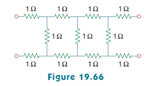
Find the impedance parameter equivalent of the network in Fig. 19.66.
Expert Solution & Answer
Want to see the full answer?
Check out a sample textbook solution
Students have asked these similar questions
5052
ми
a
JXL
000
+2
16s (wt) bi
jxc
M
100♫
ZL.
Find the Value of XL & X c
if the Circuit trans for Max.
Power to (ZL).
Choose the best answer for each:
1. What does SRAM use to store data?
。 a) Capacitors
ob) Latches
。 c) Flip-flops
od) Transistors
2. Which RAM type requires refreshing?
o a) SRAM
ob) DRAM
。 c) ROM
od) Flash
3. What type of memory retains data only while power is on?
a) ROM
。 b) EEPROM
o c) DRAM
od) Flash
4. How many addresses can a 15-bit address bus handle?
o a) 32k
•
b) 64k
o c) 16k
od) lk
5. What operation occurs when data is copied out of memory without erasing?
oa) Write
ob) Read
o c) Refresh
o d) Load
6. DRAM cells store bits using:
a) Flip-flops
。 b) Capacitors
c) Diodes
od) Resistors
7. The cache located inside the CPU is:
。 a) L2 cache
o b) LI cache
°c) ROM
od) HDD
8. SDRAM is synchronized with:
o a) Cache
ob) Data Bus
c) System Clock
od) Hard Disk
9. The bus that carries commands is called:
o a) Data Bus
b) Control Bus
o
c) Address Bus
o d) Logic Bus
10. What is the main use of SRAM?
o Disk storage
o Cache
o Main memory
o Registers
11. The smallest addressable unit in…
Q4: A cache memory is 128k × 16. How many bytes can it store?
Chapter 19 Solutions
EE 98: Fundamentals of Electrical Circuits - With Connect Access
Ch. 19.2 - Find the z parameters of the two-port network in...Ch. 19.2 - Calculate I1 and I2 in the two-port of Fig. 19.11....Ch. 19.3 - Obtain the y parameters for the T network shown in...Ch. 19.3 - Obtain the y parameters for the circuit in Fig....Ch. 19.4 - Determine the h parameters for the circuit in Fig....Ch. 19.4 - Find the impedance at the input port of the...Ch. 19.4 - For the ladder network in Fig. 19.30, determine...Ch. 19.5 - Find the transmission parameters for the circuit...Ch. 19.5 - Prob. 9PPCh. 19.6 - Determine [y] and [T] of a two-port network whose...
Ch. 19.6 - Find the z parameters of the op amp circuit in...Ch. 19.7 - Find V2/Vs in the circuit in Fig. 19.43. Figure...Ch. 19.7 - Obtain the y parameters for the network in Fig....Ch. 19.7 - Obtain the ABCD parameter representation of the...Ch. 19.8 - Obtain the h parameters for the network in Fig....Ch. 19.8 - Obtain the z parameters of the circuit in Fig....Ch. 19.9 - For the transistor amplifier of Fig. 19.60, find...Ch. 19.9 - Prob. 18PPCh. 19 - For the single-element two-port network in Fig....Ch. 19 - For the single-element two-port network in Fig....Ch. 19 - For the single-element two-port network in Fig....Ch. 19 - For the single-element two-port network in Fig....Ch. 19 - For the single-element two-port network in Fig....Ch. 19 - For the single-element two-port network in Fig....Ch. 19 - When port 1 of a two-port circuit is...Ch. 19 - A two-port is described by the following...Ch. 19 - If a two-port is reciprocal, which of the...Ch. 19 - Prob. 10RQCh. 19 - Obtain the z parameters for the network in Fig....Ch. 19 - Find the impedance parameter equivalent of the...Ch. 19 - Find the z parameters of the circuit in Fig....Ch. 19 - Using Fig. 19.68, design a problem to help other...Ch. 19 - Obtain the z parameters for the network in Fig....Ch. 19 - Compute the z parameters of the circuit in Fig....Ch. 19 - Calculate the z parameters of the circuit in Fig....Ch. 19 - Find the z parameters of the two-port in Fig....Ch. 19 - The y parameters of a network are:...Ch. 19 - Construct a two-port that realizes each of the...Ch. 19 - Determine a two-port network that is represeted by...Ch. 19 - For the circuit shown in Fig. 19.73, let z=106412...Ch. 19 - Determine the average power delivered to ZL = 5 +...Ch. 19 - For the two-port network shown in Fig. 19.75, show...Ch. 19 - For the two-port circuit in Fig. 19.76,...Ch. 19 - For the circuit in Fig. 19.77, at = 2 rad/s, z11...Ch. 19 - Prob. 17PCh. 19 - Calculate the y parameters for the two-port in...Ch. 19 - Using Fig. 19.80, design a problem to help other...Ch. 19 - Find the y parameters for the circuit in Fig....Ch. 19 - Obtain the admittance parameter equivalent circuit...Ch. 19 - Obtain the y parameters of the two-port network in...Ch. 19 - (a) Find the y parameters of the two-port in Fig....Ch. 19 - Find the resistive circuit that represents these y...Ch. 19 - Prob. 25PCh. 19 - Calculate [y] for tle two-port in Fig. 19.85.Ch. 19 - Find the y parameters for the Circuit in Fig....Ch. 19 - In the circuit of Fig. 19.65, the input port is...Ch. 19 - In the bridge circuit of Fig. 19.87, I1 = 20 A and...Ch. 19 - Find the h parameters for the networks in Fig....Ch. 19 - Determine the hybrid parameters for the network in...Ch. 19 - Using Fig. 19.90, design a problem to help other...Ch. 19 - Obtain the h parameters for the two-port of Fig....Ch. 19 - Obtain the h and g parameters of the two-port in...Ch. 19 - Determine the h parameters for the network in Fig....Ch. 19 - For the two-port in Fig. 19.94. h=16320.01S Find:...Ch. 19 - The input port of the circuit in Fig. 19.79 is...Ch. 19 - The h parameters of the two-port of Fig. 19.95...Ch. 19 - Obtain the g parameters for the wye circuit of...Ch. 19 - Using Fig. 19.97, design a problem to help other...Ch. 19 - For the two-port in Fig. 19.75, show that...Ch. 19 - The h parameters of a two-port device are given by...Ch. 19 - Find the transmission parameters for the...Ch. 19 - Using Fig. 19.99, design a problem to help other...Ch. 19 - Find the ABCD parameters for the circuit in Fig....Ch. 19 - Find the transmission parameters for the circuit...Ch. 19 - Obtain the ABCD parameters for the network in Fig....Ch. 19 - For a two-port, let A = 4, B = 30 , C = 0.1 S, and...Ch. 19 - Using impedances in the s-domain, obtain the...Ch. 19 - Derive the s-domain expression for the t...Ch. 19 - Obtain the t parameters for the network in Fig....Ch. 19 - (a) For the T network in Fig. 19.106, show that...Ch. 19 - Prob. 53PCh. 19 - Show that the transmission parameters of a...Ch. 19 - Prove that the g parameters can be obtained from z...Ch. 19 - For the network of Fig. 19.107, obtain VoVs....Ch. 19 - Given the transmission parameters T=32017 obtain...Ch. 19 - Design a problem to help other students better...Ch. 19 - Given that g=0.06S0.40.22 determine: (a) [z] (b)...Ch. 19 - Design a T network necessary to realize the...Ch. 19 - For the bridge circuit in Fig. 19.108, obtain: (a)...Ch. 19 - Find the z parameters of the op amp circuit in...Ch. 19 - Determine the z parameters of the two-port in Fig....Ch. 19 - Determine the y parameters at = 1,000 rad/s for...Ch. 19 - What is the y parameter presentation of the...Ch. 19 - In the two-port of Fig. 19.113, let y12 = y21 = 0,...Ch. 19 - If three copies of the circuit in Fig. 19.114 are...Ch. 19 - Obtain the h parameters for the network in Fig....Ch. 19 - The circuit in Fig. 19.116 may be regarded as two...Ch. 19 - For the parallel-series connection of the two...Ch. 19 - Determine the z parameters for the network in Fig....Ch. 19 - A series-parallel connection of two two-ports is...Ch. 19 - Three copies of the circuit shown in Fig. 19.70...Ch. 19 - Determine the ABCD parameters of the circuit in...Ch. 19 - For the individual two-ports shown in Fig. 19.121...Ch. 19 - Use PSpice or MultiSim to obtain the z parameters...Ch. 19 - Using PSpice or MultiSim, find the h parameters of...Ch. 19 - Obtain the h parameters at = 4 rad/s for the...Ch. 19 - Use PSpice or MultiSim to determine the z...Ch. 19 - Use PSpice or MultiSim to find the z parameters of...Ch. 19 - Repeat Prob. 19.26 using PSpice or MultiSim....Ch. 19 - Use PSpice or MultiSim to rework Prob. 19.31....Ch. 19 - Rework Prob. 19.47 using PSpice or MultiSim....Ch. 19 - Using PSpice or MultiSim, find the transmission...Ch. 19 - At =1rad/s, find the transmission parameters of...Ch. 19 - Obtain the g parameters for the network in Fig....Ch. 19 - For the circuit shown in Fig. 19.129, use PSpice...Ch. 19 - Using the y parameters, derive formulas for Zin,...Ch. 19 - A transistor has the following parameters in a...Ch. 19 - A transistor with hfe=120,hie=2khre=104,hoe=20S is...Ch. 19 - For the transistor network of Fig. 19.130,...Ch. 19 - Prob. 92PCh. 19 - Prob. 93PCh. 19 - A transistor in its common-emitter mode is...Ch. 19 - Prob. 95PCh. 19 - Prob. 96PCh. 19 - Synthesize the transfer function...Ch. 19 - A two-stage amplifier in Fig. 19.134 contains two...Ch. 19 - Assume that the two circuits in Fig. 19.135 are...
Knowledge Booster


Learn more about
Need a deep-dive on the concept behind this application? Look no further. Learn more about this topic, electrical-engineering and related others by exploring similar questions and additional content below.Similar questions
- Sketch the output of the analogue computer shown below and find its closest describing function [suppose any variable to find the DF] +1 ew2 HI e2 1.0 +21 LO SJ eo SJ ew LO 1.0 +|e1| HI -1 ew1 ek(1 + e。) |e1| k = 1+|e1| Figure V-5 Feedback Limiter Behavior ROUNDED, DUE TO DIODE NONLINEARITY LIMIT VOLTAGE 409 DIODE CONDUCTS First, write the output transaction, then draw the output wave, and then find the Describing function. I need to solve the question step by step, with an explanation of each step.arrow_forwardSketch the output of the analogue computer shown below and find its closest describing function [suppose any variable to find the DF] SJ ew2 ew₁ HI |e2| 2 LO 1.0 +21 LO -1 HI Jel 1.0+|e1| ROUNDED, DUE TO DODE NONLINEARITY LIMIT VOLTAGE DIODE CONDUCTS ew1e, -k(1+ e。) k = |e1| 1+|e1| Figure 1-5 Feedback Limiter Behavior First, write the output transaction, then draw the output wave, and then find the Describing function. I need to solve the question step by step, with an explanation of each step.arrow_forwardSketch the output of the analogue computer shown below and find its closest describing function [suppose any variable to find the DF] SJ +1 HI LO e2 1.0 +21 ew2 eo SJ ew₁ LO Jel 1.0 +|e1| HI -1 ew1 ek(1+eo) k = |e1| 1+|e1| First, write the output transaction, then draw the output wave, and then find the Describing function. I need to solve the question step by step, with an explanation of each step.arrow_forward
- Can you help me find the result of an integral 0/2 a² X + a dxarrow_forwardQ1/Sketch the root locus for the system shown in Figure 1 and find the following: a. The exact point and gain where the locus crosses the jo-axis b. The breakaway point on the real axis c. The range of K within which the system is stable d. Angles of departure and arrival R(s) + K(s²-4s +20) C(s) (s+2)(s + 4)arrow_forwardExam2 Subject: (Numerical Analysis) Class: Third Date: 27/4/2025 Time: 60 minutes Q1. For what values of k does this system of equations has no solution? (use Gauss-Jordan eliminations) kx + y + z = 1 x+ky + z = 1 x+y+kz=1arrow_forward
- Consider the Difference equation of a causal Linear time-invariant (LTI) system given by: (y(n) - 1.5y(n - 1) + 0.5y(n = 2) = x(n) a) Implement the difference equation model of this system. b) Find the system transfer function H(z). c) For an input x(n) = 8(n), determine the output response y(n). d) Verify the initial value theorem y(0) with part (c).arrow_forwardQ5B. Find the type of the controller in the following figures and use real values to find the transfer function of three of them[ Hint Pi,Pd and Lead,lag are found so put the controller with its corresponding compensator]. R₁ R₂ Rz HE C2 RA HE R₁ R2 RA とarrow_forwardQ1// Sketch the root locus for the unity feedback system. Where G(s)=)= K S3+252 +25 and find the following a. Sketch the asymptotes b. The exact point and gain where the locus crosses the jo-axis c. The breakaway point on the real axis d. The range of K within which the system is stable e. Angles of departure and arrival.arrow_forward
- Determine X(w) for the given function shown in Figure (1) by applying the differentiation property of the Fourier Transform. Figure (1) -1 x(t)arrow_forwardCan you solve a question with a drawing Determine X(w) for the given function shown in Figure (1) by applying the differentiation property of the Fourier Transform. Figure (1) -1 x(t)arrow_forwardAn inductor has a current flow of 3 A when connected to a 240 V, 60 Hz power line. The inductor has a wire resistance of 15 Find the Q of the inductorarrow_forward
arrow_back_ios
SEE MORE QUESTIONS
arrow_forward_ios
Recommended textbooks for you
 Introductory Circuit Analysis (13th Edition)Electrical EngineeringISBN:9780133923605Author:Robert L. BoylestadPublisher:PEARSON
 Delmar's Standard Textbook Of ElectricityElectrical EngineeringISBN:9781337900348Author:Stephen L. HermanPublisher:Cengage Learning
 Programmable Logic ControllersElectrical EngineeringISBN:9780073373843Author:Frank D. PetruzellaPublisher:McGraw-Hill Education
 Fundamentals of Electric CircuitsElectrical EngineeringISBN:9780078028229Author:Charles K Alexander, Matthew SadikuPublisher:McGraw-Hill Education
 Electric Circuits. (11th Edition)Electrical EngineeringISBN:9780134746968Author:James W. Nilsson, Susan RiedelPublisher:PEARSON
 Engineering ElectromagneticsElectrical EngineeringISBN:9780078028151Author:Hayt, William H. (william Hart), Jr, BUCK, John A.Publisher:Mcgraw-hill Education,
Introductory Circuit Analysis (13th Edition)
Electrical Engineering
ISBN:9780133923605
Author:Robert L. Boylestad
Publisher:PEARSON
Delmar's Standard Textbook Of Electricity
Electrical Engineering
ISBN:9781337900348
Author:Stephen L. Herman
Publisher:Cengage Learning
Programmable Logic Controllers
Electrical Engineering
ISBN:9780073373843
Author:Frank D. Petruzella
Publisher:McGraw-Hill Education
Fundamentals of Electric Circuits
Electrical Engineering
ISBN:9780078028229
Author:Charles K Alexander, Matthew Sadiku
Publisher:McGraw-Hill Education
Electric Circuits. (11th Edition)
Electrical Engineering
ISBN:9780134746968
Author:James W. Nilsson, Susan Riedel
Publisher:PEARSON
Engineering Electromagnetics
Electrical Engineering
ISBN:9780078028151
Author:Hayt, William H. (william Hart), Jr, BUCK, John A.
Publisher:Mcgraw-hill Education,
Z Parameters - Impedance Parameters; Author: Electrical Engineering Authority;https://www.youtube.com/watch?v=qoD4AoNmySA;License: Standard Youtube License