Electronics Fundamentals: Circuits, Devices & Applications
8th Edition
ISBN: 9780135072950
Author: Thomas L. Floyd, David Buchla
Publisher: Prentice Hall
expand_more
expand_more
format_list_bulleted
Concept explainers
Videos
Textbook Question
Chapter 17, Problem 9P
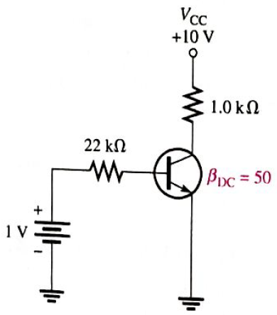
Determine
Expert Solution & Answer
Want to see the full answer?
Check out a sample textbook solution
Students have asked these similar questions
1
ezt
Evaluate Sc z² (z²+2z+2)
2πί
|z|=3 and t=constant.
dz using residue theorem if C is the circle
Find Z-1 {(z-1)²(2-2)(2-3))
2z
using residue theorem.
Please answer all
Chapter 17 Solutions
Electronics Fundamentals: Circuits, Devices & Applications
Ch. 17 - In a bipolar transistor, if the base-emitter...Ch. 17 - When a transistor is saturated. an increase in...Ch. 17 - Prob. 3TFQCh. 17 - The power gain of a CC amplifier is the same as...Ch. 17 - A class B amplifier is more efficient than a class...Ch. 17 - A JFET is always operated with the gate-source...Ch. 17 - Prob. 7TFQCh. 17 - The transconductance of a FET is the ratio of ac...Ch. 17 - Prob. 9TFQCh. 17 - The input to a feedback oscillator is only the...
Ch. 17 - The n-type regions in an npn bipolar junction...Ch. 17 - The n-region in a pnp transistor is the base...Ch. 17 - Prob. 3STCh. 17 - Prob. 4STCh. 17 - Prob. 5STCh. 17 - Alpha () is the ratio of collector current to...Ch. 17 - If the beta of a certain transistor operating in...Ch. 17 - If the base current of a transistor operating in...Ch. 17 - Prob. 9STCh. 17 - When the gate-to-source voltage of an n-channel...Ch. 17 - When a negative gate-to-source voltage is applied...Ch. 17 - Prob. 12STCh. 17 - If the capacitor from emitter to ground in a CE...Ch. 17 - When the collector resistor in a CE amplifier is...Ch. 17 - The input resistance of a CE amplifier is affected...Ch. 17 - The output signal of a CE amplifier is always in...Ch. 17 - The output signal of a common-collector amplifier...Ch. 17 - The largest theoretical voltage gain obtainable...Ch. 17 - In a class A amplifier, the output signal is...Ch. 17 - A class A amplifier conducts for 90 of input cycle...Ch. 17 - Prob. 21STCh. 17 - Feedback oscillators operate on the principle of...Ch. 17 - What is the value of IC for IE=5.34mA and IB=475A?Ch. 17 - Prob. 2PCh. 17 - Prob. 3PCh. 17 - In a certain transistor circuit, the base current...Ch. 17 - Find IB,IE, and in Figure 17-70 given that DC=0.98...Ch. 17 - The transistor in Figure 17-70 is replaced with...Ch. 17 - Prob. 7PCh. 17 - Prob. 8PCh. 17 - Determine IB,IC, and VC in Figure 17-72.Ch. 17 - For the circuit in Figure 17-73, find VB,VE,IE,IC,...Ch. 17 - In Figure 17-73, what is VCE? What are the Q-point...Ch. 17 - A transistor amplifier has a voltage gain of 50....Ch. 17 - To achieve an output of 10 V with an input of300...Ch. 17 - A 50 mV signal is applied to the base of a...Ch. 17 - Determine the voltage gain for Figure 17-74.Ch. 17 - Determine each of the dc voltages, VB,VC, and VE,...Ch. 17 - Determine the following dc values for the...Ch. 17 - Determine the following ac values for the...Ch. 17 - The amplifier in Figure 17-76 has a variable gain...Ch. 17 - If a load resistance of 600 is placed on the...Ch. 17 - Determine the voltage gain for the...Ch. 17 - What is the total input resistance in Figure...Ch. 17 - A load resistance is capacitively coupled in the...Ch. 17 - Prob. 24PCh. 17 - Determine the maximum peak output voltage and peak...Ch. 17 - The efficiency of a certain class B push-pull...Ch. 17 - Prob. 27PCh. 17 - The transistor in Figure 17-80 has a DC of 150....Ch. 17 - The VGS of ap-channel JFET is increased from 1 V...Ch. 17 - Why must the gate-to-source voltage of an...Ch. 17 - Draw the schematic symbols for n-channel and...Ch. 17 - Explain why both types of MOSFETs have an...Ch. 17 - In what mode is an n-channel D-MOSFET operating...Ch. 17 - A certain E-MOSFET has a VGS(th)=3V. What is the...Ch. 17 - For each circuit in Figure 17-81, determine VDS...Ch. 17 - Prob. 36PCh. 17 - Each E-MOSFET in Figure 17-83 has a VGS(th) of +5...Ch. 17 - Prob. 38PCh. 17 - Find the gain of each amplifier in Figure 17-85.Ch. 17 - Determine the gain of each amplifier in Figure...Ch. 17 - If the voltage gain of the amplifier portion of a...Ch. 17 - Generally describe the change required to the...Ch. 17 - Prob. 43PCh. 17 - Prob. 44PCh. 17 - Prob. 47PCh. 17 - Prob. 48PCh. 17 - Prob. 49PCh. 17 - Prob. 50PCh. 17 - Prob. 51PCh. 17 - Prob. 52PCh. 17 - Open file P17-53. Determine if the circuit is...
Knowledge Booster


Learn more about
Need a deep-dive on the concept behind this application? Look no further. Learn more about this topic, electrical-engineering and related others by exploring similar questions and additional content below.Similar questions
- find the inverse Laplace transform of X(s)= i) Re[s]> 3 ii) Re[s]<1 s+5 for (s-1)(s-2)(s-3) iii) 1arrow_forwardFor R1, what is the resistance in kΩ? For R1, what the current in mA? For R1, what is the voltage in V? For R1, what is the power in W? For R2, what is the resistance in kΩ? For R2, what the current in mA? For R2, what is the voltage in V? For R2, what is the power in W? For R3, what is the resistance in kΩ? For R3, what the current in mA? For R3, what is the voltage in V? For R3, what is the power in W? For R4, what is the resistance in kΩ? For R4, what the current in mA? For R4, what is the voltage in V? For R4, what is the power in W? For R5, what is the resistance in kΩ? For R5, what the current in mA? For R5, what is the voltage in V? For R5, what is the power in W? What is the total resistance in Ω? What is the total current in mA? What is the total voltage in V? What is the total power in W?arrow_forwardPlease answer allarrow_forward7.48 Determine the Thevenin equivalent of the circuit inFig. P7.48 at terminals (a,b), given thatVs(t) = 12cos 2500t V,Is(t) = 0.5cos(2500t −30◦) A.arrow_forward1. In the following closed-loop system, a PD controller of the form K(s + 5) is used. Design the gain K such that the system achieves an overshoot of 16%. Calculate the settling time and peak time for the PD controlled system. Compensator R(s) + E(s) Plant 1 C(s) K(s+Zc) (s+1)(s+2)(s+5)arrow_forwardFind Voarrow_forwardarrow_back_iosSEE MORE QUESTIONSarrow_forward_ios
Recommended textbooks for you
 Power System Analysis and Design (MindTap Course ...Electrical EngineeringISBN:9781305632134Author:J. Duncan Glover, Thomas Overbye, Mulukutla S. SarmaPublisher:Cengage Learning
Power System Analysis and Design (MindTap Course ...
Electrical Engineering
ISBN:9781305632134
Author:J. Duncan Glover, Thomas Overbye, Mulukutla S. Sarma
Publisher:Cengage Learning
Multistage Transistor Audio Amplifier Circuit; Author: The Organic Chemistry Tutor;https://www.youtube.com/watch?v=LJrL9N9uhkE;License: Standard Youtube License