
Electronics Fundamentals: Circuits, Devices & Applications
8th Edition
ISBN: 9780135072950
Author: Thomas L. Floyd, David Buchla
Publisher: Prentice Hall
expand_more
expand_more
format_list_bulleted
Concept explainers
Videos
Textbook Question
Chapter 17, Problem 10P
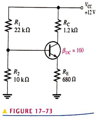
For the circuit in Figure 17-73, find
Expert Solution & Answer
Want to see the full answer?
Check out a sample textbook solution
Students have asked these similar questions
80 V
300 Ω
t = 0
500 i(t)
Vc(t)
40 nF
2,5 mH
-
Problem 1: Two-Force Equilibrium
A 12 kg traffic light is suspended by two cables
attached to a ceiling. Determine the force in Cable 1
(AB) and Cable 2 (AC). In other words, determine the
tension in each cable, assuming the system is in static
equilibrium.
B
If the Z-axis changes, what is the effect
A circularly polarized wave, traveling in the +z-direction, is received by an elliptically
polarized antenna whose reception characteristics near the main lobe are given approx-
imately by
E₁ = (2â, + jâ] f(r. 8. d)
Find the polarization loss factor PLF (dimensionless and in dB) when the incident wave
is
(a) right-hand (CW)
(b) left-hand (CCW)
An elliptically polarized wave traveling in the negative z-direction is received by a circularly polarized
antenna. The vector describing the polarization of the incident wave is given by Ei= 2ax + jay .Find the
polarization loss factor PLF (dimensionless and in dB) when the wave that would be transmitted by the
antenna is (a) right-hand CP (b) left-hand CP.
Chapter 17 Solutions
Electronics Fundamentals: Circuits, Devices & Applications
Ch. 17 - In a bipolar transistor, if the base-emitter...Ch. 17 - When a transistor is saturated. an increase in...Ch. 17 - Prob. 3TFQCh. 17 - The power gain of a CC amplifier is the same as...Ch. 17 - A class B amplifier is more efficient than a class...Ch. 17 - A JFET is always operated with the gate-source...Ch. 17 - Prob. 7TFQCh. 17 - The transconductance of a FET is the ratio of ac...Ch. 17 - Prob. 9TFQCh. 17 - The input to a feedback oscillator is only the...
Ch. 17 - The n-type regions in an npn bipolar junction...Ch. 17 - The n-region in a pnp transistor is the base...Ch. 17 - Prob. 3STCh. 17 - Prob. 4STCh. 17 - Prob. 5STCh. 17 - Alpha () is the ratio of collector current to...Ch. 17 - If the beta of a certain transistor operating in...Ch. 17 - If the base current of a transistor operating in...Ch. 17 - Prob. 9STCh. 17 - When the gate-to-source voltage of an n-channel...Ch. 17 - When a negative gate-to-source voltage is applied...Ch. 17 - Prob. 12STCh. 17 - If the capacitor from emitter to ground in a CE...Ch. 17 - When the collector resistor in a CE amplifier is...Ch. 17 - The input resistance of a CE amplifier is affected...Ch. 17 - The output signal of a CE amplifier is always in...Ch. 17 - The output signal of a common-collector amplifier...Ch. 17 - The largest theoretical voltage gain obtainable...Ch. 17 - In a class A amplifier, the output signal is...Ch. 17 - A class A amplifier conducts for 90 of input cycle...Ch. 17 - Prob. 21STCh. 17 - Feedback oscillators operate on the principle of...Ch. 17 - What is the value of IC for IE=5.34mA and IB=475A?Ch. 17 - Prob. 2PCh. 17 - Prob. 3PCh. 17 - In a certain transistor circuit, the base current...Ch. 17 - Find IB,IE, and in Figure 17-70 given that DC=0.98...Ch. 17 - The transistor in Figure 17-70 is replaced with...Ch. 17 - Prob. 7PCh. 17 - Prob. 8PCh. 17 - Determine IB,IC, and VC in Figure 17-72.Ch. 17 - For the circuit in Figure 17-73, find VB,VE,IE,IC,...Ch. 17 - In Figure 17-73, what is VCE? What are the Q-point...Ch. 17 - A transistor amplifier has a voltage gain of 50....Ch. 17 - To achieve an output of 10 V with an input of300...Ch. 17 - A 50 mV signal is applied to the base of a...Ch. 17 - Determine the voltage gain for Figure 17-74.Ch. 17 - Determine each of the dc voltages, VB,VC, and VE,...Ch. 17 - Determine the following dc values for the...Ch. 17 - Determine the following ac values for the...Ch. 17 - The amplifier in Figure 17-76 has a variable gain...Ch. 17 - If a load resistance of 600 is placed on the...Ch. 17 - Determine the voltage gain for the...Ch. 17 - What is the total input resistance in Figure...Ch. 17 - A load resistance is capacitively coupled in the...Ch. 17 - Prob. 24PCh. 17 - Determine the maximum peak output voltage and peak...Ch. 17 - The efficiency of a certain class B push-pull...Ch. 17 - Prob. 27PCh. 17 - The transistor in Figure 17-80 has a DC of 150....Ch. 17 - The VGS of ap-channel JFET is increased from 1 V...Ch. 17 - Why must the gate-to-source voltage of an...Ch. 17 - Draw the schematic symbols for n-channel and...Ch. 17 - Explain why both types of MOSFETs have an...Ch. 17 - In what mode is an n-channel D-MOSFET operating...Ch. 17 - A certain E-MOSFET has a VGS(th)=3V. What is the...Ch. 17 - For each circuit in Figure 17-81, determine VDS...Ch. 17 - Prob. 36PCh. 17 - Each E-MOSFET in Figure 17-83 has a VGS(th) of +5...Ch. 17 - Prob. 38PCh. 17 - Find the gain of each amplifier in Figure 17-85.Ch. 17 - Determine the gain of each amplifier in Figure...Ch. 17 - If the voltage gain of the amplifier portion of a...Ch. 17 - Generally describe the change required to the...Ch. 17 - Prob. 43PCh. 17 - Prob. 44PCh. 17 - Prob. 47PCh. 17 - Prob. 48PCh. 17 - Prob. 49PCh. 17 - Prob. 50PCh. 17 - Prob. 51PCh. 17 - Prob. 52PCh. 17 - Open file P17-53. Determine if the circuit is...
Knowledge Booster


Learn more about
Need a deep-dive on the concept behind this application? Look no further. Learn more about this topic, electrical-engineering and related others by exploring similar questions and additional content below.Similar questions
- Medium 1 is a lossless dielectric (ε₁=ε,ε, μ₁=μ₁, σ₁=0) Medium 2 is a lossless dielectric (ε=&&₂, μ=μ₁, σ₁=0) [бг Мо о = = 0] [2 Mo σ₂ = 0] E₁ (z) = Ele² + Пe+jB₁²] E2 (z) = E Te² and tot = constant 1. For the case εr1 = 1, &r2= 16, E₁x=1 V/m and a frequency f = 750 MHz determine: λι = n₁ = 22 = n2= r = T= 2. The magnitude |E1 tot (z)| will show an interference pattern in region 1 as: E˜(z)=E,{1+Te®®]e¯MS =E||{1+Te^^^^\]e=##} | = |E|+Texp(j) For an incident field E₁x=1 V/m SKETCH the magnitude of E1 tot (z)| and |E20 (z) on the graph below. Plot the values at 2/4 increments and sketch between. What is the SWR?arrow_forwardPlease don't use AIarrow_forwardPlease don't use AIarrow_forward
- 3) In the ideal autotransformer circuit shown below find 11, 12 and lo. Find the average power delivered to the load. (hint: write KVL for both sides) 20/30° V(+ 2-1602 200 turns V₂ 10 + j40 Ω 80 turns V₁arrow_forward11-2) Now consider that white noise (i.e., noise with a PSD that is constant with frequency) is introduced in the channel of the system described in the previous problem. An ideal low pass filter is used at the receiver input to reduce the noise as much as possible, while transmitting the desired signal. (a) By what factor should the cutoff frequency of the noise reduction filter be reduced in the 16-PAM case, compared to binary? (b) By what factor will the noise power at the decision circuit be reduced in the 16-PAM case? (c) By what factor will the noise amplitude at the decision circuit be reduced in the 16-PAM case? (d) To obtain the same symbol error rate for 16-PAM as for binary, how should the minimum level spacing for 16-PAM compare to binary? (e) If the 16-PAM level spacing is adjusted according to part (d) above, by what factor will the average signal power be increased in the 16-PAM case, compared to binary?arrow_forward11-1) similar to Lathi & Ding, Prob. P.6.7-5 Data at a bit rate Rb must be transmitted using either binary NRZ polar signaling or 16-ary PAM NRZ polar signaling. (a) By what factor will the symbol rate be reduced in the 16-PAM case? (b) By what factor will bandwidth required from the (lowpass) channel be reduced in the 16-PAM case? (c) Assuming the minimum spacing between pulse levels must be the same in both cases, by what factor will the average power be increased in the 16-PAM case? [Hint: take the pulse amplitudes to be ±A in the binary case, and ±A, ±3A, ±5A,..., ±154, and recall that scaling pulse amplitude by a factor k scales the pulse energy by a factor R². Assume that the data is random, so that all 16 levels are equally likely, and that the same pulse shape is used in both cases.] Warning: Solutions to the textbook problem that are posted online are mostly wrong. Work it out for yourself.arrow_forward
- 11-3) similar to Lathi & Ding, Prob. P.6.8-1 Consider the carrier modulator shown in the figure below, which transmits a binary carrier signal. The baseband generator uses polar NRZ signaling with rectangular pulses. The data rate is 8 Mbit/s. (a) If the modulator generates a binary PSK signal, what is the bandwidth of the modulated output? (b) If the modulator generates FSK with the difference fel - fco = 6 MHz (cf. Fig 6.32c), determine the modulated signal bandwidth. Binary data source Baseband signal generator Modulated output Modulator N-E---arrow_forwardFor the circuit shown, find (i) closed-loop voltage gain (ii) Z i of the circuit (iii) f_max. The slew rate is 0.6V/us. ((write your answer in Kilo ohm)) 2Vpp R ww 20 kQ R₁ ww 200 ΚΩ 9+18 V - 18 V 10 kn R₁₂ ΚΩ ((write your answer in KHz))arrow_forwardillustrate the phenomenon of phase reversal in CE amplifier i- When signal current =OA, so IB-8uA ii- When input signal reaches positive peak, so IB=16uA ii- When input signal reaches negative peak, so IB=4uA R₁ www + Vcc = 12V Rc=6kn 16 A 8 μA 4 μА 0 www RE ẞ = 100 VCarrow_forward
- In the circuit shown, find the voltage gain. Given that ẞ = 80 and input resistance Rin=2kQ. SIGNAL +10 V Rc=6kn 4-2 210arrow_forwardFor the transistor amplifier shown, R₁-11kQ, R2=6kQ, Rc=2kQ, RE-3kQ and R₁=2k0. (i) Draw d.c. load line (ii) Determine the DC operating point (iii) Draw a.c. load line. Assume V_BE = 0.7 V. and determine the new operating point + Vcc = 15 V RC Cc Cin R1 wwwwww wwwww R₁₂ RE CE RLarrow_forwardthe first part is the second part write your answer such as: (AND, OR, INVERTER, NAND, NOR) D₁ AK D, R₁ B K First Part? the third part is , and the total are R4 R7 Output R5 R₁ T R6 R3 -UBB Second Part? Third Part? Total?arrow_forward
arrow_back_ios
SEE MORE QUESTIONS
arrow_forward_ios
Recommended textbooks for you
 Introductory Circuit Analysis (13th Edition)Electrical EngineeringISBN:9780133923605Author:Robert L. BoylestadPublisher:PEARSON
 Delmar's Standard Textbook Of ElectricityElectrical EngineeringISBN:9781337900348Author:Stephen L. HermanPublisher:Cengage Learning
 Programmable Logic ControllersElectrical EngineeringISBN:9780073373843Author:Frank D. PetruzellaPublisher:McGraw-Hill Education
 Fundamentals of Electric CircuitsElectrical EngineeringISBN:9780078028229Author:Charles K Alexander, Matthew SadikuPublisher:McGraw-Hill Education
 Electric Circuits. (11th Edition)Electrical EngineeringISBN:9780134746968Author:James W. Nilsson, Susan RiedelPublisher:PEARSON
 Engineering ElectromagneticsElectrical EngineeringISBN:9780078028151Author:Hayt, William H. (william Hart), Jr, BUCK, John A.Publisher:Mcgraw-hill Education,
Introductory Circuit Analysis (13th Edition)
Electrical Engineering
ISBN:9780133923605
Author:Robert L. Boylestad
Publisher:PEARSON
Delmar's Standard Textbook Of Electricity
Electrical Engineering
ISBN:9781337900348
Author:Stephen L. Herman
Publisher:Cengage Learning
Programmable Logic Controllers
Electrical Engineering
ISBN:9780073373843
Author:Frank D. Petruzella
Publisher:McGraw-Hill Education
Fundamentals of Electric Circuits
Electrical Engineering
ISBN:9780078028229
Author:Charles K Alexander, Matthew Sadiku
Publisher:McGraw-Hill Education
Electric Circuits. (11th Edition)
Electrical Engineering
ISBN:9780134746968
Author:James W. Nilsson, Susan Riedel
Publisher:PEARSON
Engineering Electromagnetics
Electrical Engineering
ISBN:9780078028151
Author:Hayt, William H. (william Hart), Jr, BUCK, John A.
Publisher:Mcgraw-hill Education,
Multistage Transistor Audio Amplifier Circuit; Author: The Organic Chemistry Tutor;https://www.youtube.com/watch?v=LJrL9N9uhkE;License: Standard Youtube License