
Videos
The parameters of the TIL NAND circuit in Figure 17.24 are:
(a)
The value of the base and the collector current in each of the transistor.
Answer to Problem 17.9EP
The value of the currents are
Explanation of Solution
Calculation:
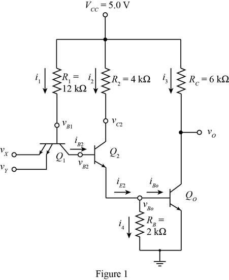
The given diagram is shown in Figure 1.
The expression for the voltage
Substitute
The second transistor and the transistor at the output are both cut off, then the base voltage
Substitute
The expression for the value of the current
Substitute
The expression to determine the value of the base current
Substitute
The transistor two and the output transistor are cutoff, therefore the value of the current are given by,
The expression for the value of the current
Conclusion:
Therefore, the value of the currents are
(b)
The value of the base and the collector current in each of the transistor.
Answer to Problem 17.9EP
The value of the currents are
Explanation of Solution
Calculation:
The input transistor is biased with inverse active mode when the input voltage is
The expression for the voltage
Substitute
The expression to determine the value of the collector voltage is given by,
Substitute
The expression to determine the value of the current
Substitute
The expression to determine the value of the base current
Substitute
The expression to determine the value of the current
Substitute
The expression to determine the value of the collector current
Substitute
The expression to determine the value of the current
Substitute
The expression to determine the value of the base current
Substitute
The expression to determine the value of the base current
Substitute
The expression to determine the value of the current
Substitute
The expression to determine the value of the current
Substitute
The expression to determine the value of the current
Substitute
Conclusion:
Therefore, the value of the currents are
Want to see more full solutions like this?
Chapter 17 Solutions
Microelectronics: Circuit Analysis and Design


- 23bcarrow_forwardDraw the small-signal equivalent circuit of a single transistor amplifier given in figure B1b. Assume the current source to be ideal. Determine the Open-loop transfer function, pole frequency and gain-bandwidth product all in terms of transistor parameters 9m, To and CL. If the load capacitance is 1pF and the necessary unity gain frequency is 600MHz, find the gm for this transistor. V₁ V₁ CLarrow_forward23baarrow_forward
 Introductory Circuit Analysis (13th Edition)Electrical EngineeringISBN:9780133923605Author:Robert L. BoylestadPublisher:PEARSON
 Delmar's Standard Textbook Of ElectricityElectrical EngineeringISBN:9781337900348Author:Stephen L. HermanPublisher:Cengage Learning
 Programmable Logic ControllersElectrical EngineeringISBN:9780073373843Author:Frank D. PetruzellaPublisher:McGraw-Hill Education
 Fundamentals of Electric CircuitsElectrical EngineeringISBN:9780078028229Author:Charles K Alexander, Matthew SadikuPublisher:McGraw-Hill Education
 Electric Circuits. (11th Edition)Electrical EngineeringISBN:9780134746968Author:James W. Nilsson, Susan RiedelPublisher:PEARSON
 Engineering ElectromagneticsElectrical EngineeringISBN:9780078028151Author:Hayt, William H. (william Hart), Jr, BUCK, John A.Publisher:Mcgraw-hill Education,