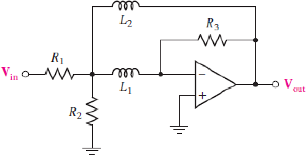
For the circuit in Fig. 15.57, (a) determine the transfer function H(s) = Vout/Vin in terms of circuit parameters R1, R2, R3, L1, and L2; (b) determine the magnitude and phase of the transfer function at ω = 0, 3 × 10³ rad/s, and as ω → ∞ for the case where circuit values are R1 = 2 kΩ, R2 = 2 kΩ, R3 = 20 kΩ, L1 = 2 H, and L2 = 2 H.
FIGURE 15.57

(a)
The transfer function
Answer to Problem 7E
The transfer function
Explanation of Solution
Given data:
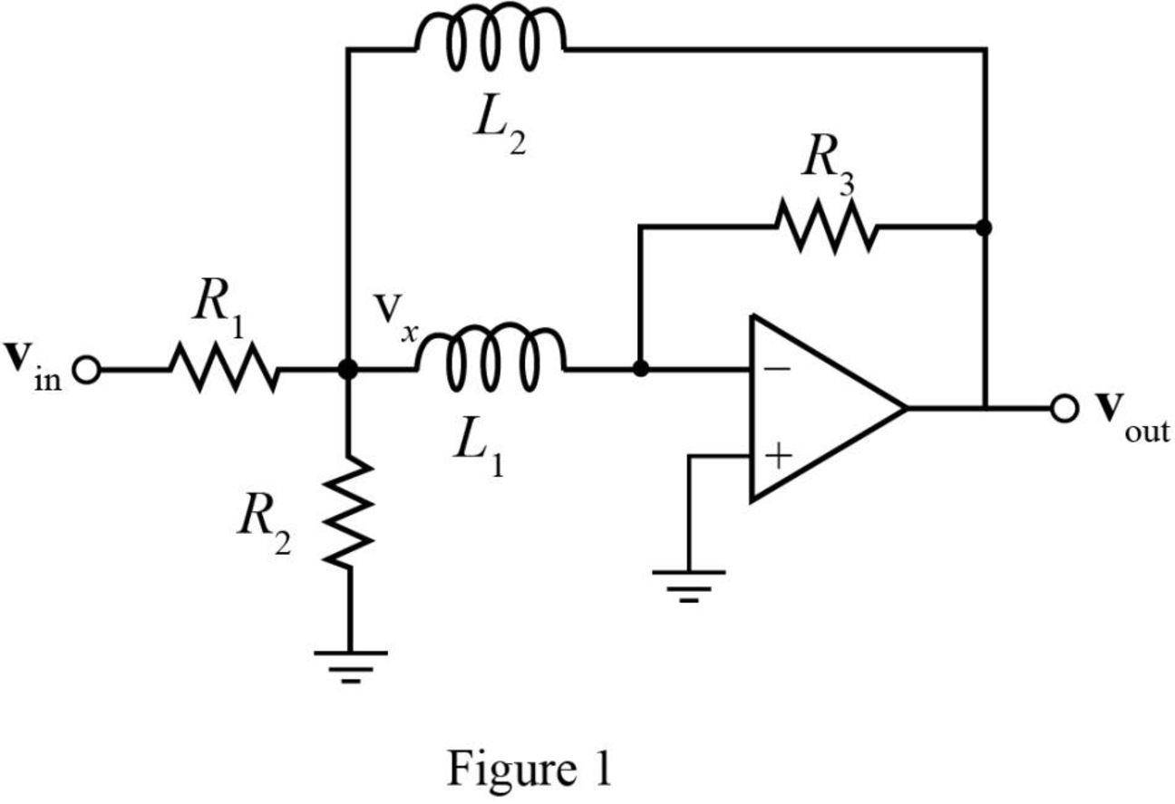
The required diagram is shown in Figure 1.

Calculation:
Assign the node intersecting the two resistors
The KCL equation at node
The KCL equation at node
Here,
Simplifying the equation (2) as,
The transfer function
Substitute
Substitute
Conclusion:
Therefore, the transfer function
(b)
The magnitude of transfer function
Answer to Problem 7E
The magnitude of transfer function
Explanation of Solution
Given data:
The resistance
The resistance
The resistance
The inductance
The inductance
The angular frequency
The angular frequency
The angular frequency
Calculation:
The conversion of
The conversion of
The conversion of
The magnitude of transfer function
The phase of transfer function
Substitute
Substitute
The magnitude of transfer function
The phase of transfer function
Substitute
Substitute
The magnitude of transfer function
The phase of transfer function
Substitute
Substitute
Conclusion:
Therefore, the magnitude of transfer function
Want to see more full solutions like this?
Chapter 15 Solutions
ENGINEERING CIRCUIT...(LL)>CUSTOM PKG.<
Additional Engineering Textbook Solutions
Database Concepts (8th Edition)
Mechanics of Materials (10th Edition)
Starting Out with Programming Logic and Design (5th Edition) (What's New in Computer Science)
SURVEY OF OPERATING SYSTEMS
Elementary Surveying: An Introduction To Geomatics (15th Edition)
Java: An Introduction to Problem Solving and Programming (8th Edition)
- Q4. Give the reasons for the following 1. In AC machines drives, the frequency modulation index should be integer regardless the value of switching frequency. 2. Variable de link voltage is adopted in inverter operating in square wave operation mode 3. Practical values of switch utilization factor is different from theoretical values 4. In three-phase inverter with my is odd and multiple of 3, the even and tripplen harmonics are zero. 5. The PSC-PWM is attractive for the modular multilevel converterarrow_forwardQ6.B. Answer the following questions 1. Does the steady state load current in a half bridge inverter has an average value and what is the adverse effect of the average current component? 2. Can the LPF of single phase bridge inverter based on bipolar PWM be used with single phase bridge inverter based on unipolar PWM? Explainarrow_forwardQ3. Answer the following questions T 1. Compared to the bipolar voltage-switching scheme, the unipolar scheme is "effectively" doubling the switching frequency. Explain the statement's meaning and how this effect can be generated. 2. What are the properties of a good power switch, and what are its basic ratings? 3. What are the objectives of any PWM strategy for three-phase inverters? 4. Why is the current control PWM rectifier in the dq rotating reference frame preferred over the abc reference frame? 5. Define the switch utilization factor. Show how this factor can be calculated for different single-phase inverters for square wave operation mode at the maximum rated output.arrow_forward
- Q1.B. Explain output control by voltage cancellation in a single-phase inverter. What are the advantages over square wave operation?arrow_forwardQ3.B. What is the problem of three-phase HW rectifier and how can be resolved?arrow_forwardQ3-consider the unity feedback system shown below: a.Evaluate general formula of ess? b.Calculate the steady state error of the closed loop system due to R(s) unit step input, D(s)=0]? c.Calculate the steady-state response when D(s) and ramp and R(s)=0?arrow_forward
- - = 400KHZ. Q1. In a Boost converter, L = 25 μH, Vin = 12 V, D = 0.4, P = 25 W, and fs (i) if the output load is changing. Calculate the critical value of the output load P,below which the converter will enter the discontinuous conduction mode of operation. Assume the total turn-on loss is equal to 2 W. (ii) Assuming the input voltage fluctuates from 10 V to 14 V and the output voltage is regulated to 20 V. Calculate the critical value of the inductance L below which this Boost converter will enter the discontinuous conduction mode of operation at P = 5 W. (iii) Draw the waveforms for inductor voltage, inductor current, and the capacitor current for this Boost converter at the output load that causes it to operate at the border of continuous and discontinuous modes. vd tow 77 N₂ AT 22 1-1arrow_forwardDon't use ai to answer I will report you answerarrow_forwardAnswer the following questions: 1- Write radiation resistance (R.) equation for infinitesimal dipole antenna. 2- Write the angle expression form of first null beam width (FNBW) for 2/2 dipole. 3- Define the Directivity of antenna. 4- Write radar cross section equation. 5- Write the input impedance (Z) expression of lossless transmission line.arrow_forward
 Introductory Circuit Analysis (13th Edition)Electrical EngineeringISBN:9780133923605Author:Robert L. BoylestadPublisher:PEARSON
 Delmar's Standard Textbook Of ElectricityElectrical EngineeringISBN:9781337900348Author:Stephen L. HermanPublisher:Cengage Learning
 Programmable Logic ControllersElectrical EngineeringISBN:9780073373843Author:Frank D. PetruzellaPublisher:McGraw-Hill Education
 Fundamentals of Electric CircuitsElectrical EngineeringISBN:9780078028229Author:Charles K Alexander, Matthew SadikuPublisher:McGraw-Hill Education
 Electric Circuits. (11th Edition)Electrical EngineeringISBN:9780134746968Author:James W. Nilsson, Susan RiedelPublisher:PEARSON
 Engineering ElectromagneticsElectrical EngineeringISBN:9780078028151Author:Hayt, William H. (william Hart), Jr, BUCK, John A.Publisher:Mcgraw-hill Education,


