
(a)
To derive: the expression for the voltage transfer function
(a)
Explanation of Solution
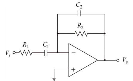
Given:

Calculation:
Redraw the given circuit in s -domain as
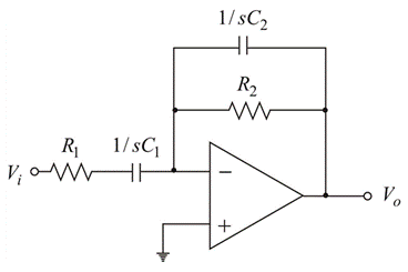
From the circuit,
Now the transfer function is
Hence
Thus, the required voltage transfer function is
Conclusion:
Thus, the required voltage transfer function is
(b)
To find: The value of
(b)
Answer to Problem 15.18P
The required values are
Explanation of Solution
Given:
Magnitude of the mid band gain is 50
Cut-off frequency
Cut-off frequency
Calculation:
Consider
The magnitude of the voltage transfer function is given by
Given
To determine the cut-off frequency
For
For
Let us consider
The equation (1) becomes,
From equation (2),
Substituting equation (5) in equation (4),
Substitute the values of
Hence the roots are obtained as
Since
Now, substitute the value of
Hence, by substituting the values
Further simplify as
Given
Therefore, the required resistor value is
Now
Therefore, the required capacitor
Conclusion:
Therefore, the required values are
Want to see more full solutions like this?
Chapter 15 Solutions
MICROELECT. CIRCUIT ANALYSIS&DESIGN (LL)

- I have uploaded the rules, please explain step by step and which rule you have appliedarrow_forwardUsing the CCS Compiler method to solve this question Write a PIC16F877A program that flash ON the 8-LED's connected to port-B by using two switches connected to port-D (Do & D₁) as shown in figure below, according to the following scenarios: (Hint: Use 500ms delay for each case with 4MHz frequency) 1. When Do=1 then B₁,B3,B7 are ON. 2. When Do 0 then Bo,B2, B4, B5, B6 are ON. 3. When D₁=1 then B4,B,,B6,B7 are ON. 4. When D₁-0 then Bo,B1,B2,B3 are ON.arrow_forwardUse the ramp generator circuit in Fig. B2a to generate the waveform shown in Fig. B2b. Write four equations relating resistors R1, R2, R3, capacitor C and voltages Vs, VR and VA.to the waveform parameters T₁, T, Vcm and Vm- If R = R2 = R3, R₁ = 2R, C = 1 nF, Vcm = 2 V and Vm = 1 V, T₁ = 2 μs and T = 10 μs solve for the values of R, Vs, VR and VA using your equations from part a(i). VR C +VA R3 V₂ Vo мат R1 VsO+ V₁ R₂ Figure B2a Vout Vcm+Vm Vcm Vcm-Vm 0 T₁ T 2T time Figure B2barrow_forward
- The circuit in Figure B1a is a common analogue circuit block. Explain why you would need such a circuit. Draw another circuit in which you use the current flowing in this loop to bias a common source amplifier. This circuit is not ideal for standard CMOS technologies due to threshold shift. Why? Draw an improved version of this circuit to make it better. VDD (W)P MA M3. (), REF (쁜)~ M₁ M2 lout 시~ Rsarrow_forward23bcarrow_forwardDraw the small-signal equivalent circuit of a single transistor amplifier given in figure B1b. Assume the current source to be ideal. Determine the Open-loop transfer function, pole frequency and gain-bandwidth product all in terms of transistor parameters 9m, To and CL. If the load capacitance is 1pF and the necessary unity gain frequency is 600MHz, find the gm for this transistor. V₁ V₁ CLarrow_forward
 Introductory Circuit Analysis (13th Edition)Electrical EngineeringISBN:9780133923605Author:Robert L. BoylestadPublisher:PEARSON
 Delmar's Standard Textbook Of ElectricityElectrical EngineeringISBN:9781337900348Author:Stephen L. HermanPublisher:Cengage Learning
 Programmable Logic ControllersElectrical EngineeringISBN:9780073373843Author:Frank D. PetruzellaPublisher:McGraw-Hill Education
 Fundamentals of Electric CircuitsElectrical EngineeringISBN:9780078028229Author:Charles K Alexander, Matthew SadikuPublisher:McGraw-Hill Education
 Electric Circuits. (11th Edition)Electrical EngineeringISBN:9780134746968Author:James W. Nilsson, Susan RiedelPublisher:PEARSON
 Engineering ElectromagneticsElectrical EngineeringISBN:9780078028151Author:Hayt, William H. (william Hart), Jr, BUCK, John A.Publisher:Mcgraw-hill Education,