
Concept explainers
Videos
A.
Worst case output voltages
A.
Answer to Problem D14.47P
Worst case output voltages are
Explanation of Solution
Given:
The given circuit is:
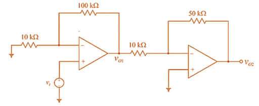
As
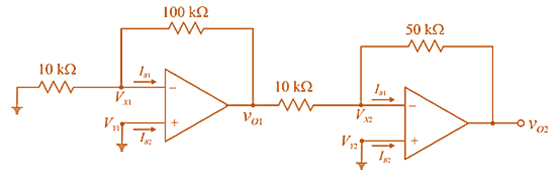
For first op-amp
Also
Now, KCL at input node
For second op-amp
Also
Now, KCL at input node
B.
To design:
Input bias current compensation circuit.
B.
Explanation of Solution
Given:
A simple compensation circuit can minimize the effect of bias currents in op-amp.
Consider the sketch ofinput bias current compensation circuit as,
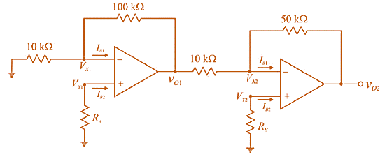
Now, determine
For first op-amp:
KCL at non-inverting node,
As,
Therefore,
KCL at inverting node,
Putting
Now,
If
For second op-amp:
KCL at non-inverting node,
As,
Therefore,
KCL at inverting node,
Putting
Now,
If
Want to see more full solutions like this?
Chapter 14 Solutions
Microelectronics: Circuit Analysis and Design


- A Three-phase, 12 pole, Y-connected alternator has 108 slots and 14 conductors per slot. The windings are (5/6 th) pitched. The flux per pole is 57 mWb distributed sinusoidally over the pole. If the machine runs at 500 r.p.m., determine the following: (a) The frequency of the generated e.m.f., (b) The distribution factor, (c) The pitch factor, and (d) The phase and line values of the generated e.m.f.?arrow_forwardTwo 3-ph, 6.6 kV, Y-connected, alternators supply a load of 3000 kW at 0.8 p.f. lagging. The synchronou impedance per phase of machine A is (0.5+110) and that of machine B is (0.4 +J12) . The excitation of machine A adjusted so that it delivers 150 A. The load is shared equally between the machines. Determine the armature curre p.f., induced e.m.f., and load angle of each machine?arrow_forwardName the circuit below? The output voltage is initially zero and the pulse width is 200 μs. Find the Vout and draw the output waveform? +2.5 V V 247 -2.5 V C 0.01 F Ri W 10 ΚΩarrow_forward
- Please work outarrow_forwardFind Vfinal when Vs up and Vs V. Which LED will light in each case? Red or Green? Justify your answers. Fill the table below. Vs 8 ΚΩ Vos Χρι + 3 ΚΩ www 6 ΚΩ ww 4 ΚΩ Yo www Vo Vec-12 V Nol V final Vm w 3 ΚΩ 5 V 38 ΚΩ R= 1 kQ V -12 V Red LED Green LED Vs Vo Vfinal Which LED is ON? Varrow_forwardCircuits help please solve and explain. Question in images providedarrow_forward
- + V 6.2 A 1.2 A S R 4 Ω Find the source voltage Vs 0.8 Aarrow_forwardDetermine i(t) for t≥ 0 given that the circuit below had been in steady state for a long time prior to t = 0. Also, I₁ = 1 5 A, R₁ =22, R2 =10 Q2, R3 = 32, R4 =7 2, and L=0.15 H. Also fill the table. m L ww R2 t = 0 R₁ 29 R3 R4 Time 0 iL(t) 0 8arrow_forwardPlease help explain this problemarrow_forward
- + P = 16 W w w P = 8 W I R₁ R2 E = RT=322 1- Determine R1, R2, E ΙΩarrow_forward+ 30 V = - 20 V + R 2- Use KVL to find the voltage V - V + + 8 Varrow_forwardFind the Thévenin equivalent circuit for the portions of the networks in Figure external to the elements between points a and b. a R₁ 2002 I = 0.1 A 0° Xc : 32 Ω R2 = 6802 20 Ω фъarrow_forward
 Introductory Circuit Analysis (13th Edition)Electrical EngineeringISBN:9780133923605Author:Robert L. BoylestadPublisher:PEARSON
 Delmar's Standard Textbook Of ElectricityElectrical EngineeringISBN:9781337900348Author:Stephen L. HermanPublisher:Cengage Learning
 Programmable Logic ControllersElectrical EngineeringISBN:9780073373843Author:Frank D. PetruzellaPublisher:McGraw-Hill Education
 Fundamentals of Electric CircuitsElectrical EngineeringISBN:9780078028229Author:Charles K Alexander, Matthew SadikuPublisher:McGraw-Hill Education
 Electric Circuits. (11th Edition)Electrical EngineeringISBN:9780134746968Author:James W. Nilsson, Susan RiedelPublisher:PEARSON
 Engineering ElectromagneticsElectrical EngineeringISBN:9780078028151Author:Hayt, William H. (william Hart), Jr, BUCK, John A.Publisher:Mcgraw-hill Education,