
Videos
A.
Output voltage due to input bias current and worst case output voltage.
A.
Answer to Problem 14.50P
Output voltage due to input bias current is
Explanation of Solution
Given:
The given circuit is:
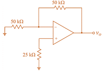
Input bias current
Input offset current
Let the general circuit with input bias currents
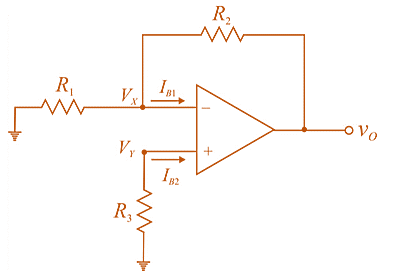
Now, using superposition determine
For
The output voltage due to
For
Since,
The output voltage due to
So, the vet output voltage due to both
If
So, the output voltage due to bias current
Now putting the values,
Now, for worst case output
As,
And
Adding (5) and (6)
From (5)
For
For
Assume
For the given circuit
Putting the values in (3)
So, including the effect of input offset current, the worst case output voltage is
B.
Output voltage due to input bias current and worst case output voltage.
B.
Answer to Problem 14.50P
Output voltage due to input bias current is
Explanation of Solution
Given:
The given circuit is:
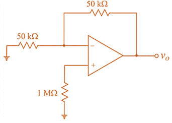
Input bias current
Input offset current
Considering equation 4.
Now, for worst case output voltage
Assume
For the given circuit
Putting the values in (3)
So, including the effect of input offset current, the worst case output voltage is
Want to see more full solutions like this?
Chapter 14 Solutions
Microelectronics: Circuit Analysis and Design


- Pick up the correct answer along with evde ce for explanation 2. Taking into account cost, most of the high-voltage transmission lines are A. Underground. B. Overhead C. Either of the above D. None of the aber 3. If the maximum load is equal to plant capacity. The plant capacity factor is: A. 1 B. zero C. >1 D. <1 5. Sum of continuous ratings of all the equipment connected to electric power system is defined as: A. Maximum demand B. Connected load 6. Cables have more effective in B. Capacitance C. Daily average load than over head transmission lines C. Resistance D. Load variation D. All of the abov 100% A. Inductance 7. By which of the following methods string efficiency can be equal A. Using a guard ring B. Equal insulator voltage C. Using long cross arm D. Non of them -10. If the spacing between the conductors is decrease, the inductance of the line will be: A. Increase B. decreases C. Not effected D. Non of them 12. If the length of a transmission line increases, its inductance is…arrow_forwardDon't use ai to answer I will report you answer Use the method of superposition to find...arrow_forwardDon't use ai to answer I will report you answerarrow_forward
- Don't use ai to answer I will report you answerarrow_forwardQ1: What is the orientation of voltage regulation value (positive or negative) of alternator loaded by capacitive load? Explain the effect of armature reaction on voltage regulation for this load? Draw the load characteristics of alternator for capacitive, inductive, and inductive loads?arrow_forwardI what happend if can IY = 125 lead, IB = 125 unity IR=89.91 unity IB = 125-> Lag 0.8 Iy=125 IB 36.86 lag 0.8 Ir< 36-86 IN=IR+IN+IB FR 89.910+125<-120-36.86+1252+120 -36.86arrow_forward
- Manual solution only, no Al usedarrow_forwardLook up the dislocation-induced energy levels in silicon and GaAs - cite your sources. a. Sketch them in the band gap. b. When are each of them most active? c. Are dislocations more detrimental in Si or GaAs? d. What is the threshold of dislocation density that each semiconductor can handle?arrow_forwardQ1: In a material for which o 9 s/m and e, -4, the electric field intensity E = 50 sin 8*10'1 V/m. Find: a. The conduction and displacement current densities. b. The frequency at which the conduction current is half the displacement current.arrow_forward
- Q2: The circular loop conductor lies in the Z-0 plane, has a radius of 40 cm and a resistance of 40 Q. Given B-0.9 sin 5°10' ta, Determine a. The induced voltage b. Currentarrow_forwardQW= 2x + y²+2z, x-In(). y= r² + In(rs) and z = 2r. Find W, and W,arrow_forwardQ1: F(x,y) ycosiy) + xe Find: fe-fry-fy and farrow_forward
 Introductory Circuit Analysis (13th Edition)Electrical EngineeringISBN:9780133923605Author:Robert L. BoylestadPublisher:PEARSON
 Delmar's Standard Textbook Of ElectricityElectrical EngineeringISBN:9781337900348Author:Stephen L. HermanPublisher:Cengage Learning
 Programmable Logic ControllersElectrical EngineeringISBN:9780073373843Author:Frank D. PetruzellaPublisher:McGraw-Hill Education
 Fundamentals of Electric CircuitsElectrical EngineeringISBN:9780078028229Author:Charles K Alexander, Matthew SadikuPublisher:McGraw-Hill Education
 Electric Circuits. (11th Edition)Electrical EngineeringISBN:9780134746968Author:James W. Nilsson, Susan RiedelPublisher:PEARSON
 Engineering ElectromagneticsElectrical EngineeringISBN:9780078028151Author:Hayt, William H. (william Hart), Jr, BUCK, John A.Publisher:Mcgraw-hill Education,