
Videos
(a)
Design a circuit which produces a transfer function of
(a)
Explanation of Solution
Given data:
The given transfer function is,
Calculation:
The transfer function of the circuit is,
The above transfer function has a zero at
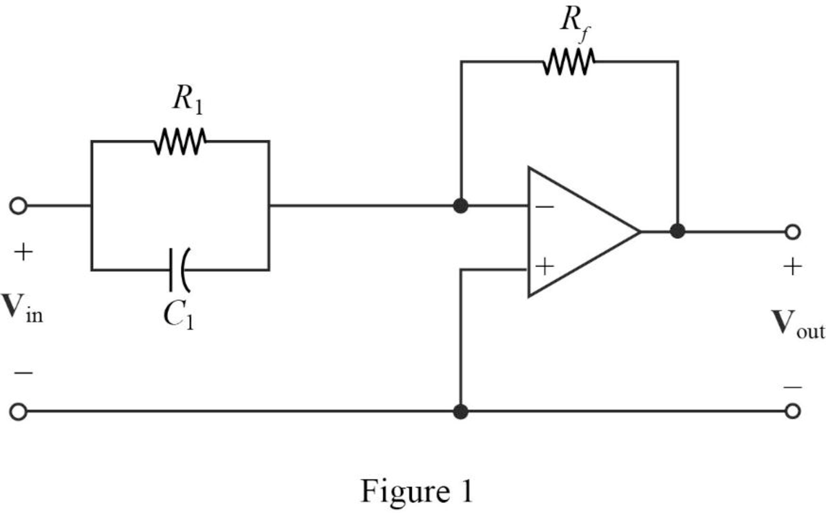
The Figure 14.39 (b) in the textbook, that shows a cascade two stages of the circuit with a zero at
For a single zero,
Substitute
Consider the value of
Substitute
Transfer function:
The input impedance of the cascaded circuit in Figure 1 is,
Then, write the Formula for the transfer function for the cascaded two stage amplifier.
Substitute
Thus, the transfer function for
Substitute 1 for
Completing the design by letting
If the input will be inverted, add an inverting amplifier with gain of 1 to provide the transfer function as follows.
Thus, the final design of the circuit is,
Conclusion:
Thus, a circuit is designed which produces a transfer function of
(b)
Design a circuit which produces a transfer function of
(b)
Explanation of Solution
Given data:
The given transfer function is,
Calculation:
The transfer function of the circuit is,
The above transfer function has pole at
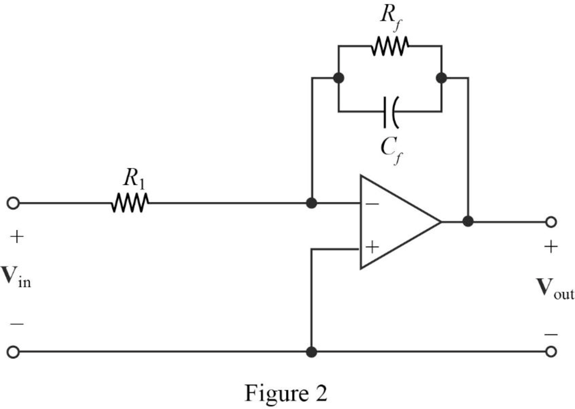
The Figure 14.39 (a) in the textbook, that shows a cascade two stages of the circuit with pole at
For pole
Substitute
Let arbitrarily consider
Substitute
Transfer function:
Find the feedback impedance of the cascaded circuit in Figure 2.
Write the formula for the transfer function of the cascaded circuit in Figure 2 as follows
Substitute
Therefore, consider the transfer function
Substitute 1 for
Completing the design by letting
If the input will be inverted, add an inverting amplifier with gain of 1 to provide the transfer function as follows.
Thus, the final design of the circuit is,
Conclusion:
Thus, a circuit is designed which produces a transfer function of
(c)
Design a circuit which produces a transfer function of
(c)
Explanation of Solution
Given data:
The given transfer function is,
Calculation:
The transfer function of the circuit is,
For the above transfer function, it has a zero at
Refer to Figure 1 in Part (a), that shows a cascade two stages of the circuit with a zero at
For a single zero,
Substitute
Let arbitrarily consider
Substitute
Consider the same circuit shown in Figure 1 and the transfer function as in a cascaded circuit,
Substitute 1 for
Completing the design by letting
Thus, the final design of the circuit is,
The given transfer function has a pole at
Refer to Figure 2 in Part (b), that shows a cascade two stages of the circuit with pole at
For pole
Substitute
Let arbitrarily consider
Substitute
The above equation becomes,
Consider the same circuit shown in Figure 2 and the transfer function as in a cascaded circuit,
Substitute 2 for
Completing the design by letting
Thus, the final design of the circuit is,
Therefore, the overall transfer function of the cascaded circuit is,
Substitute
Conclusion:
Thus, a circuit is designed which produces a transfer function of
Want to see more full solutions like this?
Chapter 14 Solutions
ENGINEERING CIRCUIT...(LL)>CUSTOM PKG.<


- Calculate the torque developed by the motor if Field. excitation is so adjusted as to make the back e.mif twice the applied voltage and α = 16°, Neglecting losses for a 3-phasi 150 KW 2300 V, 50 Hz, 1000 rpm salient Pole synchronous motor has Xd=32 52/Phase and Xy = 2052/phase. 7arrow_forwardASSIGNMENT NO. 6 1. Consider the circuit below with C = 0.02 uF, Ri 100 kr and Rf = 470 k2. The input waveform has T = 0.5 ms and Vp = 8 V. Under steady state conditions, determine the peak-to-peak value of the output voltage.arrow_forwardAn RLC circuit is build with a 250 microfarad capacitor 10 mH inductor an a 15 ohms resistance in series. It isoperated with a Voltage source of Frequency of 400HZ and maximum voltage 12V. Find the angular frequency of thesource. Find the reactance of each circuit element. Find the impedance and the peak current. Find the phase factortheta between the current and the voltage source. Write the current and voltage of the circuit as a function of time.Draw an approximate V vs t and I vs t diagram. Find the resonance frequencyarrow_forward
- The project conditions are:The project functionality will be provided as per the project description suppliedbelow.You must present/demonstrate the project as a group, at the given time,andwithin a given time limit ( 20 mins ).A soft copy of all project documents is required before you The program functionality should be as follows:• Upon entering the “run” mode all counters/timers must be reset (use the first scan bit).• When students scan RFID cards, the opening motor automatically opens the door and closing motor closes it after a 5 second wait.• The current number of students should be counted by incrementing/decrementing as students enter or leave the classroom. • The number of students entering the classroom is counted using a reflective sensor, while the number leaving is counted using a fiber optic sensor. The count should be displayed in the decimal tag "Total no of students”.• The maximum number of students in the classroom is 20, and when the classroom is occupied by the…arrow_forwardSolve this problem and show all of the workarrow_forward1. The circuit below has R1 =R2 R3 = 10 kohms and R4 = 2.5 kohms. For V1 = 5 V and V2 = 4.2 V, determine: (a) Vx (b) lx (c) VR (d) Va (e) Vb (1) Vo ww Rarrow_forward
- I need help with this problem and an step by step explanation of the solution from the image described below. (Introduction to Signals and Systems)arrow_forwardI need help with this problem and an step by step explanation of the solution from the image described below. (Introduction to Signals and Systems)arrow_forwardI need help with this problem and an step by step explanation of the solution from the image described below. (Introduction to Signals and Systems)arrow_forward
 Introductory Circuit Analysis (13th Edition)Electrical EngineeringISBN:9780133923605Author:Robert L. BoylestadPublisher:PEARSON
 Delmar's Standard Textbook Of ElectricityElectrical EngineeringISBN:9781337900348Author:Stephen L. HermanPublisher:Cengage Learning
 Programmable Logic ControllersElectrical EngineeringISBN:9780073373843Author:Frank D. PetruzellaPublisher:McGraw-Hill Education
 Fundamentals of Electric CircuitsElectrical EngineeringISBN:9780078028229Author:Charles K Alexander, Matthew SadikuPublisher:McGraw-Hill Education
 Electric Circuits. (11th Edition)Electrical EngineeringISBN:9780134746968Author:James W. Nilsson, Susan RiedelPublisher:PEARSON
 Engineering ElectromagneticsElectrical EngineeringISBN:9780078028151Author:Hayt, William H. (william Hart), Jr, BUCK, John A.Publisher:Mcgraw-hill Education,