Concept explainers
Videos
A balanced, positive-sequence wye-connected source has Van = 240
- (a) Calculate the line currents if ZAB = 40 + j15 Ω, ZBC = 60 Ω, ZCA = 18 − jl2 Ω.
- (b) Find the complex power supplied by the source.
a.
Calculate the line currents for the described circuit using PSpice.
Answer to Problem 48P
The value for the line currents
Explanation of Solution
Given data:
The phase voltage is
The transmission line impedance is
The value of the impedances
Formula used:
Write the formulae for the conversion of delta connected impedances to star connected impedances.
Here,
Write the expression for reactance of the inductor.
Here,
Write the expression for reactance of the capacitor.
Here,
Calculation:
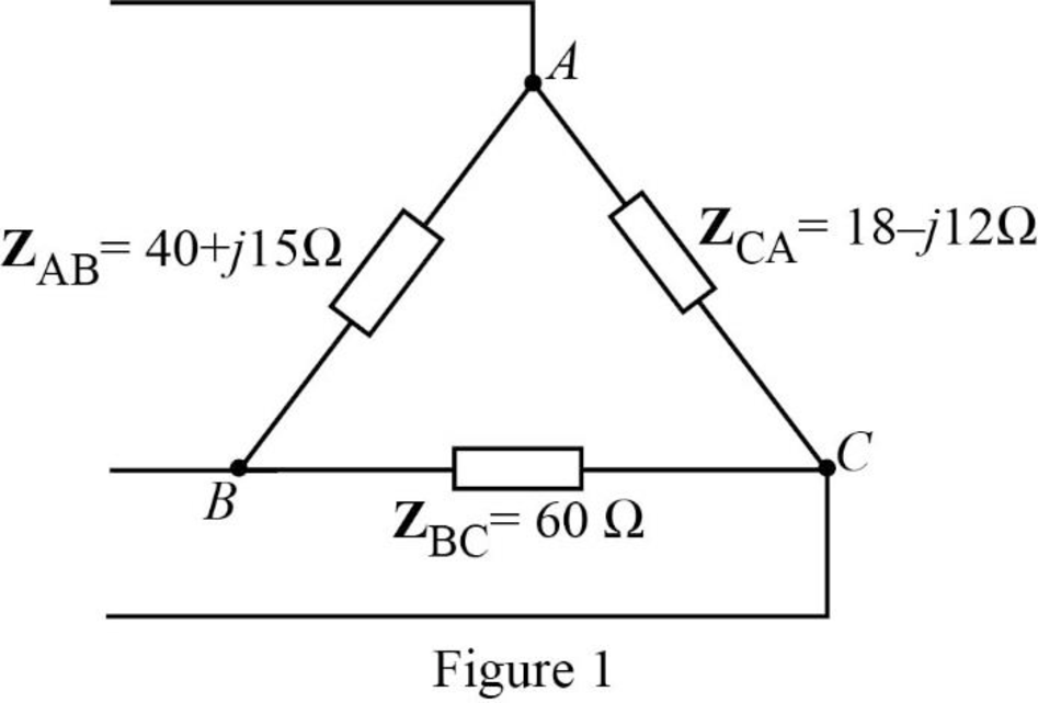
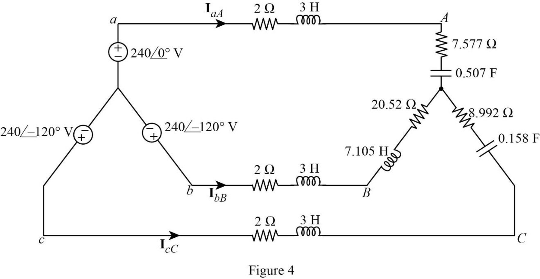
The given unbalanced delta connected load is shown in Figure 1.
Substitute
Substitute
Substitute
The transformed circuit is shown in Figure 2.
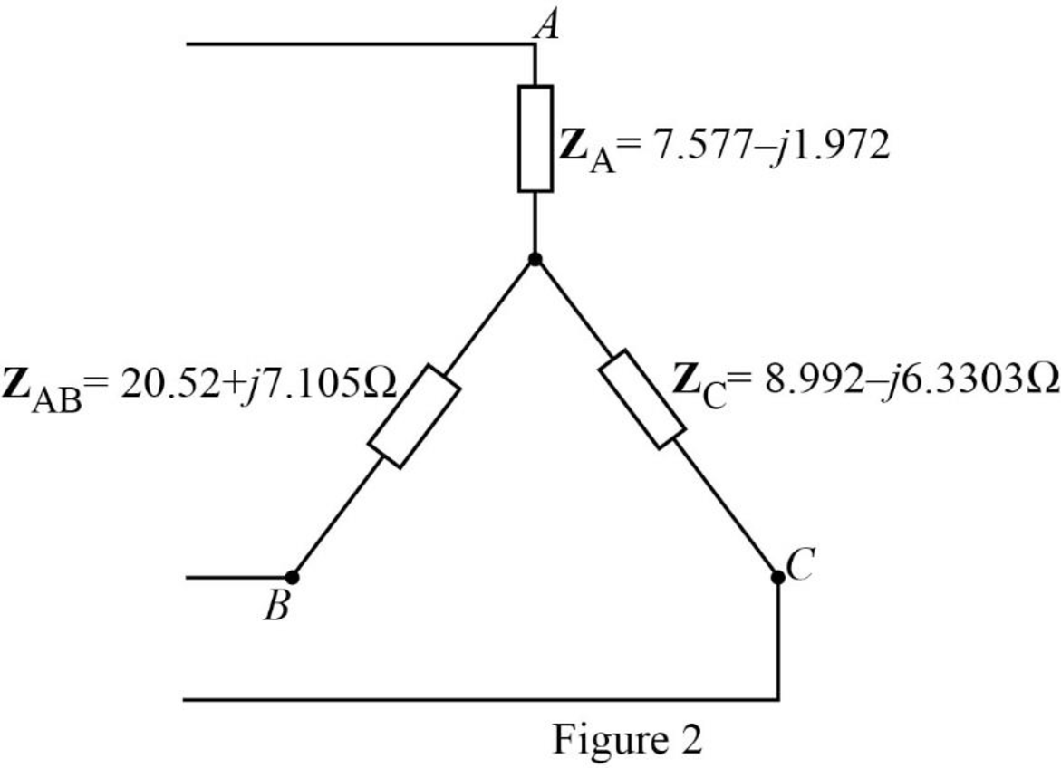
The given balanced wye-connected source supplies the unbalanced delta connected load is shown in Figure 3.
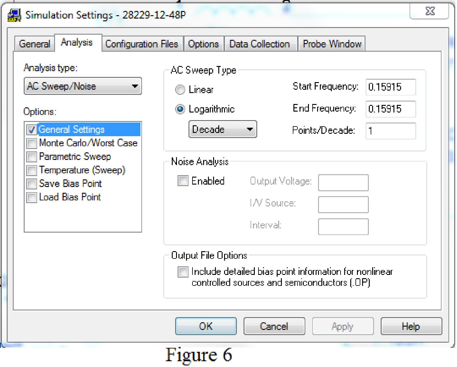
Let us assume that the value of the angular frequency,
Calculate the frequency as follows.
Substitute
Substitute
Substitute
Substitute
The time domain representation of Figure 3 is shown in Figure 4.
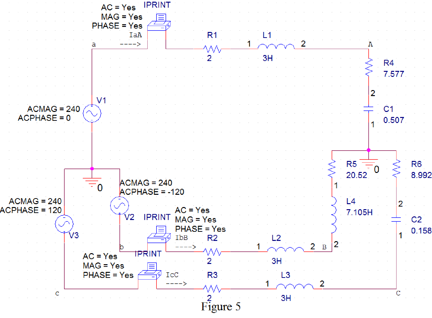
PSpice Simulation:
Draw Figure 4 in PSpice as shown in Figure 5.
Provide the simulation setting as shown in Figure 6.
The obtained results are given below.
FREQ IM(V_PRINT1) IP(V_PRINT1)
1.592E-01 2.492E+01 -6.124E+00
FREQ IM(V_PRINT2) IP(V_PRINT2)
1.592E-01 9.723E+00 -1.442E+02
FREQ IM(V_PRINT3) IP(V_PRINT3)
1.592E-01 2.094E+01 1.365E+02
The obtained line currents are given below.
Conclusion:
Thus, the value for the line currents
b.
Calculate the total complex power supplied by the source.
Answer to Problem 48P
The total complex power supplied by the source is
Explanation of Solution
Calculation:
Write the expression for complex power delivered by source
Substitute
Write the expression for complex power delivered by source
Substitute
Write the expression for complex power delivered by source
Substitute
Write the expression for total complex power supplied by the source.
Substitute
Conclusion:
Thus, the total complex power supplied by the source is
Want to see more full solutions like this?
Chapter 12 Solutions
EBK FUNDAMENTALS OF ELECTRIC CIRCUITS
Additional Engineering Textbook Solutions
Modern Database Management
Vector Mechanics for Engineers: Statics and Dynamics
Mechanics of Materials (10th Edition)
Degarmo's Materials And Processes In Manufacturing
Java How to Program, Early Objects (11th Edition) (Deitel: How to Program)
Starting Out With Visual Basic (8th Edition)


- 2. Using the approximate method, hand sketch the Bode plot for the following transfer functions. a) H(s) = 10 b) H(s) (s+1) c) H(s): = 1 = +1 100 1000 (s+1) 10(s+1) d) H(s) = (s+100) (180+1)arrow_forwardQ4: Write VHDL code to implement the finite-state machine described by the state Diagram in Fig. 1. Fig. 1arrow_forward1. Consider the following feedback system. Bode plot of G(s) is shown below. Phase (deg) Magnitude (dB) -50 -100 -150 -200 0 -90 -180 -270 101 System: sys Frequency (rad/s): 0.117 Magnitude (dB): -74 10° K G(s) Bode Diagram System: sys Frequency (rad/s): 36.8 Magnitude (dB): -99.7 System: sys Frequency (rad/s): 20 Magnitude (dB): -89.9 System: sys Frequency (rad/s): 20 Phase (deg): -143 System: sys Frequency (rad/s): 36.8 Phase (deg): -180 101 Frequency (rad/s) a) Determine the range of K for which the closed-loop system is stable. 102 10³ b) If we want the gain margin to be exactly 50 dB, what is value for K we should choose? c) If we want the phase margin to be exactly 37°, what is value of K we should choose? What will be the corresponding rise time (T) for step-input? d) If we want steady-state error of step input to be 0.6, what is value of K we should choose?arrow_forward
- : Write VHDL code to implement the finite-state machine/described by the state Diagram in Fig. 4. X=1 X=0 solo X=1 X=0 $1/1 X=0 X=1 X=1 52/2 $3/3 X=1 Fig. 4 X=1 X=1 56/6 $5/5 X=1 54/4 X=0 X-O X=O 5=0 57/7arrow_forwardQuestions: Q1: Verify that the average power generated equals the average power absorbed using the simulated values in Table 7-2. Q2: Verify that the reactive power generated equals the reactive power absorbed using the simulated values in Table 7-2. Q3: Why it is important to correct the power factor of a load? Q4: Find the ideal value of the capacitor theoretically that will result in unity power factor. Vs pp (V) VRIPP (V) VRLC PP (V) AT (μs) T (us) 8° pf Simulated 14 8.523 7.84 84.850 1000 29.88 0.866 Measured 14 8.523 7.854 82.94 1000 29.85 0.86733 Table 7-2 Power Calculations Pvs (mW) Qvs (mVAR) PRI (MW) Pay (mW) Qt (mVAR) Qc (mYAR) Simulated -12.93 -7.428 9.081 3.855 12.27 -4.84 Calculated -12.936 -7.434 9.083 3.856 12.32 -4.85 Part II: Power Factor Correction Table 7-3 Power Factor Correction AT (us) 0° pf Simulated 0 0 1 Measured 0 0 1arrow_forwardQuestions: Q1: Verify that the average power generated equals the average power absorbed using the simulated values in Table 7-2. Q2: Verify that the reactive power generated equals the reactive power absorbed using the simulated values in Table 7-2. Q3: Why it is important to correct the power factor of a load? Q4: Find the ideal value of the capacitor theoretically that will result in unity power factor. Vs pp (V) VRIPP (V) VRLC PP (V) AT (μs) T (us) 8° pf Simulated 14 8.523 7.84 84.850 1000 29.88 0.866 Measured 14 8.523 7.854 82.94 1000 29.85 0.86733 Table 7-2 Power Calculations Pvs (mW) Qvs (mVAR) PRI (MW) Pay (mW) Qt (mVAR) Qc (mYAR) Simulated -12.93 -7.428 9.081 3.855 12.27 -4.84 Calculated -12.936 -7.434 9.083 3.856 12.32 -4.85 Part II: Power Factor Correction Table 7-3 Power Factor Correction AT (us) 0° pf Simulated 0 0 1 Measured 0 0 1arrow_forward
- electric plants. Prepare the load schedulearrow_forwardelectric plants Draw the column diagram. Calculate the voltage drop. by hand writingarrow_forwardelectric plants. Draw the lighting, socket, telephone, TV, and doorbell installations on the given single-story project with an architectural plan by hand writingarrow_forward
 Power System Analysis and Design (MindTap Course ...Electrical EngineeringISBN:9781305632134Author:J. Duncan Glover, Thomas Overbye, Mulukutla S. SarmaPublisher:Cengage Learning