Videos
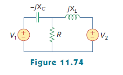
Using Fig. 11.74, design a problem to help other students better understand the conservation of AC power.
Design a problem to make the better understand of conservation of AC power.
Explanation of Solution
Problem design:
In Figure 11.74, consider the value of capacitive reactance
Formula used:
Write the expression to find the complex power.
Here,
Write the expression for the impedance
Here,
R is the value of resistance, and
X is the value of reactance.
Calculation:
Refer to Figure 11.74 in the textbook.
The given circuit is modified as shown in Figure 1.
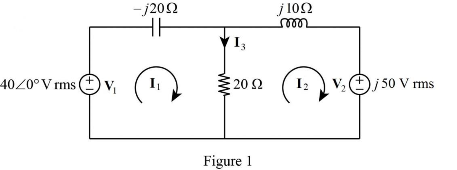
In Figure 1, apply Kirchhoff’s voltage law for loop 1 as follows.
In Figure 1, apply Kirchhoff’s voltage law for loop 2 as follows.
Put equation (3) and (4) in matrix form as follows,
Evaluate the determinant
Evaluate the determinant
Evaluate the determinant
In Figure 1, the current
Substitute
The magnitude of current
In Figure 2, the current
Substitute
The magnitude of current
The current
Substitute
The magnitude of current
The complex power absorbed by the
Substitute
From Figure (1), the impedance of capacitance is,
The complex power absorbed by the capacitor is,
Substitute
The complex power absorbed by the resistor is,
Substitute
From Figure (1), the impedance of inductance is,
The complex power absorbed by the inductor is,
Substitute
The complex power absorbed by the
Substitute
Therefore, the complex power absorbed by the
Conclusion:
Thus, a problem is designed and solved for the better understand of conservation of AC power.
Want to see more full solutions like this?
Chapter 11 Solutions
EBK FUNDAMENTALS OF ELECTRIC CIRCUITS


- A plane wave propagating in the +z direction in medium 1 is normally incident to medium 2 located at the z=0 plane as below. Both mediums are general, characterized by ( ε i, Hi, σ¡ ). [ ει μη σ] Ex [ ει μη ση ] Ex tot E₁₂ (z) = E'₁e¹² -122 E(z) = Ee+ E₁₁₁² E₁x z=0 1. Specify the electric field reflection coefficient г and transmission coefficient T: E ΓΔ E E TA EL 2. Show that T=1+г. Can the transmitted electric field amplitude in region 2 be LARGER than the incident electric field amplitude? 3. Determine expressions for P₁AV'(z), PIAV'(z) and P2AV'(z) (note the sign for the reflected power direction should be (-z).arrow_forward2) In the ideal transformer circuit shown below find Vo and the complex power supplied by the source. 292 www b 1:4 16 Ω ww + + 240/0° V rms -12492arrow_forward3) In the ideal autotransformer circuit shown below find 11, 12 and lo. Find the average power delivered to the load. (hint: write KVL for both sides) 20/30° V(+ 2-1602 200 turns V₂ 10 + j40 Ω 80 turns V₁arrow_forward
- 1) Find Vo in the following circuit. Assume the mesh currents are clockwise. ΠΩ Ω ΖΩ ww 1Ω ww 24/0° (± 6 Ω j4 Ω 1Ω +arrow_forwardPlease show all stepsarrow_forward11-3) similar to Lathi & Ding, Prob. P.6.8-1 Consider the carrier modulator shown in the figure below, which transmits a binary carrier signal. The baseband generator uses polar NRZ signaling with rectangular pulses. The data rate is 8 Mbit/s. (a) If the modulator generates a binary PSK signal, what is the bandwidth of the modulated output? (b) If the modulator generates FSK with the difference fel - fco = 6 MHz (cf. Fig 6.32c), determine the modulated signal bandwidth. Binary data source Baseband signal generator Modulated output Modulator N-E---arrow_forward
- Choose the best answer for each: 1. What does SRAM use to store data? 。 a) Capacitors ob) Latches 。 c) Flip-flops od) Transistors 2. Which RAM type requires refreshing? o a) SRAM ob) DRAM 。 c) ROM od) Flash 3. What type of memory retains data only while power is on? a) ROM 。 b) EEPROM o c) DRAM od) Flash 4. How many addresses can a 15-bit address bus handle? o a) 32k • b) 64k o c) 16k od) lk 5. What operation occurs when data is copied out of memory without erasing? oa) Write ob) Read o c) Refresh o d) Load 6. DRAM cells store bits using: a) Flip-flops 。 b) Capacitors c) Diodes od) Resistors 7. The cache located inside the CPU is: 。 a) L2 cache o b) LI cache °c) ROM od) HDD 8. SDRAM is synchronized with: o a) Cache ob) Data Bus c) System Clock od) Hard Disk 9. The bus that carries commands is called: o a) Data Bus b) Control Bus o c) Address Bus o d) Logic Bus 10. What is the main use of SRAM? o Disk storage o Cache o Main memory o Registers 11. The smallest addressable unit in…arrow_forwardQ4: A cache memory is 128k × 16. How many bytes can it store?arrow_forwardSketch the output of the analogue computer shown below and find its closest describing function [suppose any variable to find the DF] +1 ew2 HI e2 1.0 +21 LO SJ eo SJ ew LO 1.0 +|e1| HI -1 ew1 ek(1 + e。) |e1| k = 1+|e1| Figure V-5 Feedback Limiter Behavior ROUNDED, DUE TO DIODE NONLINEARITY LIMIT VOLTAGE 409 DIODE CONDUCTS First, write the output transaction, then draw the output wave, and then find the Describing function. I need to solve the question step by step, with an explanation of each step.arrow_forward
 Introductory Circuit Analysis (13th Edition)Electrical EngineeringISBN:9780133923605Author:Robert L. BoylestadPublisher:PEARSON
 Delmar's Standard Textbook Of ElectricityElectrical EngineeringISBN:9781337900348Author:Stephen L. HermanPublisher:Cengage Learning
 Programmable Logic ControllersElectrical EngineeringISBN:9780073373843Author:Frank D. PetruzellaPublisher:McGraw-Hill Education
 Fundamentals of Electric CircuitsElectrical EngineeringISBN:9780078028229Author:Charles K Alexander, Matthew SadikuPublisher:McGraw-Hill Education
 Electric Circuits. (11th Edition)Electrical EngineeringISBN:9780134746968Author:James W. Nilsson, Susan RiedelPublisher:PEARSON
 Engineering ElectromagneticsElectrical EngineeringISBN:9780078028151Author:Hayt, William H. (william Hart), Jr, BUCK, John A.Publisher:Mcgraw-hill Education,