EBK FUNDAMENTALS OF ELECTRIC CIRCUITS
6th Edition
ISBN: 8220102801448
Author: Alexander
Publisher: YUZU
expand_more
expand_more
format_list_bulleted
Concept explainers
Videos
Textbook Question
Chapter 10, Problem 7P
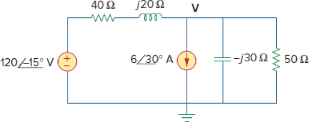
Use nodal analysis to find V in the circuit of Fig. 10.56.
Expert Solution & Answer
Want to see the full answer?
Check out a sample textbook solution
Students have asked these similar questions
A3 m long cantilever ABC is built-in at A, partially supported at B, 2 m from A,
with a force of 10 kN and carries a vertical load of 20 kN at C. A uniformly distributed
bad of 5 kN/m is also applied between A and B. Determine
(a) the values of the vertical reaction and built-in moment at A and
(b) the deflection of the free end C of the cantilever,
Develop an expression for the slope of the beam at any position and hence plot a slope diagram.
E = 208GN / (m ^ 2) and 1 = 24 * 10 ^ - 6 * m ^ 4
7. Consider the following feedback system with a proportional controller.
K
G(s)
The plant transfer function is given by
G(s) =
10
(s + 2)(s + 10)
You want the system to have a damping ratio of 0.3 for unit step response. What is the
value of K you need to choose to achieve the desired damping ratio? For that value of
K, find the steady-state error for ramp input and settling time for step input.
Hint: Sketch the root locus and find the point in the root locus that intersects with z =
0.3 line.
Create the PLC ladder logic diagram
for the logic gate circuit displayed in
Figure 7-35. The pilot light red (PLTR)
output section has three inputs: PBR,
PBG, and SW. Pushbutton red (PBR)
and pushbutton green (PBG) are inputs
to an XOR logic gate. The output of the
XOR logic gate and the inverted switch
SW) are inputs to a two-input AND
logic gate. These inputs generate the
pilot light red (PLTR) output.
The two-input AND logic gate output
is also fed into a two-input NAND logic
PBR
PBG
SW
TSW
PLTR
Figure 7-35. Logic gate circuit for Example 7-3.
PLTW
Goodheart-Willcox Publisher
gate. The temperature switch (TSW) is the other input to the NAND logic gate. The output generated from
the NAND logic gate is labeled pilot light white (PLTW).
Chapter 10 Solutions
EBK FUNDAMENTALS OF ELECTRIC CIRCUITS
Ch. 10.2 - Using nodal analysis, find v1 and v2 is in the...Ch. 10.2 - Calculate V1 and V2 in the circuit shown in Fig....Ch. 10.3 - Find Io in Fig. 10.8 using mesh analysis. Figure...Ch. 10.3 - Figure 10.11 For Practice Prob. 10.4. Calculate...Ch. 10.4 - Find current Io in the circuit of Fig. 10.8 using...Ch. 10.4 - Calculate vo in the circuit of Fig. 10.15 using...Ch. 10.6 - Determine the Norton equivalent of the circuit in...Ch. 10.7 - Find vo and io in the op amp circuit of Fig....Ch. 10.7 - Obtain the closed-loop gain and phase shift for...Ch. 10.8 - Use PSpice to obtain vo and io in the circuit of...
Ch. 10.8 - Obtain Vx and Ix in the circuit depicted in Fig....Ch. 10.9 - Determine the equivalent capacitance of the op amp...Ch. 10.9 - In the Wien-bridge oscillator circuit in Fig....Ch. 10 - The voltage Vo across the capacitor in Fig. 10.43...Ch. 10 - The value of the current Io in the circuit of Fig....Ch. 10 - Using nodal analysis, the value of Vo in the...Ch. 10 - In the circuit of Fig. 10.46, current i(t) is: (a)...Ch. 10 - Refer to the circuit in Fig. 10.47 and observe...Ch. 10 - For the circuit in Fig. 10.48, the Thevenin...Ch. 10 - In the circuit of Fig. 10.48, the Thevenin voltage...Ch. 10 - Refer to the circuit in Fig. 10.49. The Norton...Ch. 10 - Figure 10.49 For Review Questions 10.8 and 10.9....Ch. 10 - PSpice can handle a circuit with two independent...Ch. 10 - Determine i in the circuit of Fig. 10.50. Figure...Ch. 10 - Using Fig. 10.51, design a problem to help other...Ch. 10 - Determine vo in the circuit of Fig. 10.52. Figure...Ch. 10 - Compute vo(t) in the circuit of Fig. 10.53. Figure...Ch. 10 - Find io in the circuit of Fig. 10.54.Ch. 10 - Determine Vx in Fig. 10.55. Figure 10.55 For Prob....Ch. 10 - Use nodal analysis to find V in the circuit of...Ch. 10 - Use nodal analysis to find current io in the...Ch. 10 - Use nodal analysis to find vo in the circuit of...Ch. 10 - Use nodal analysis to find vo in the circuit of...Ch. 10 - Using nodal analysis, find io(t) in the circuit in...Ch. 10 - Using Fig. 10.61, design a problem to help other...Ch. 10 - Determine Vx in the circuit of Fig. 10.62 using...Ch. 10 - Calculate the voltage at nodes 1 and 2 in the...Ch. 10 - Solve for the current I in the circuit of Fig....Ch. 10 - Use nodal analysis to find Vx in the circuit shown...Ch. 10 - By nodal analysis, obtain current Io in the...Ch. 10 - Use nodal analysis to obtain Vo in the circuit of...Ch. 10 - Obtain Vo in Fig. 10.68 using nodal analysis.Ch. 10 - Refer to Fig. 10.69. If vs (t) = Vm sin t and vo...Ch. 10 - For each of the circuits in Fig. 10.70, find Vo/Vi...Ch. 10 - For the circuit in Fig. 10.71, determine Vo/Vs....Ch. 10 - Using nodal analysis obtain V in the circuit of...Ch. 10 - Design a problem to help other students better...Ch. 10 - Solve for io in Fig. 10.73 using mesh analysis....Ch. 10 - Use mesh analysis to find current io in the...Ch. 10 - Using mesh analysis, find I1 and I2 in the circuit...Ch. 10 - In the circuit of Fig. 10.76, determine the mesh...Ch. 10 - Using Fig. 10.77, design a problem help other...Ch. 10 - Use mesh analysis to find vo in the circuit of...Ch. 10 - Use mesh analysis to determine current Io in the...Ch. 10 - Determine Vo and Io in the circuit of Fig. 10.80...Ch. 10 - Compute I in Prob. 10.15 using mesh analysis....Ch. 10 - Use mesh analysis to find Io in Fig. 10.28 (for...Ch. 10 - Calculate Io in Fig. 10.30 (for Practice Prob....Ch. 10 - Compute Vo in the circuit of Fig. 10.81 using mesh...Ch. 10 - Use mesh analysis to find currents I1, I2, and I3...Ch. 10 - Using mesh analysis, obtain Io in the circuit...Ch. 10 - Find I1, I2, I3, and Ix in the circuit of Fig....Ch. 10 - Find io in the circuit shown in Fig. 10.85 using...Ch. 10 - Find vo for the circuit in Fig. 10.86, assuming...Ch. 10 - Using Fig. 10.87, design a problem to help other...Ch. 10 - Using the superposition principle, find ix in the...Ch. 10 - Use the superposition principle to obtain vx in...Ch. 10 - Use superposition to find i(t) in the circuit of...Ch. 10 - Solve for vo(t) in the circuit of Fig. 10.91 using...Ch. 10 - Determine io in the circuit of Fig. 10.92, using...Ch. 10 - Find io in the circuit of Fig. 10.93 using...Ch. 10 - Using source transformation, find i in the circuit...Ch. 10 - Using Fig. 10.95, design a problem to help other...Ch. 10 - Use source transformation to find Io in the...Ch. 10 - Use the concept of source transformation to find...Ch. 10 - Rework Prob. 10.7 using source transformation. Use...Ch. 10 - Find the Thevenin and Norton equivalent circuits...Ch. 10 - For each of the circuits in Fig. 10.99, obtain...Ch. 10 - Using Fig. 10.100, design a problem to help other...Ch. 10 - For the circuit depicted in Fig. 10.101, find the...Ch. 10 - Calculate the output impedance of the circuit...Ch. 10 - Find the Thevenin equivalent of the circuit in...Ch. 10 - Using Thevenins theorem, find vo in the circuit of...Ch. 10 - Obtain the Norton equivalent of the circuit...Ch. 10 - For the circuit shown in Fig. 10.107, find the...Ch. 10 - Using Fig. 10.108, design a problem to help other...Ch. 10 - At terminals a-b, obtain Thevenin and Norton...Ch. 10 - Find the Thevenin and Norton equivalent circuits...Ch. 10 - Find the Thevenin equivalent at terminals ab in...Ch. 10 - For the integrator shown in Fig. 10.112, obtain...Ch. 10 - Using Fig. 10.113, design a problem to help other...Ch. 10 - Find vo in the op amp circuit of Fig. 10.114....Ch. 10 - Compute io(t) in the op amp circuit in Fig. 10.115...Ch. 10 - If the input impedance is defined as Zin = Vs/Is,...Ch. 10 - Evaluate the voltage gain Av = Vo/Vs in the op amp...Ch. 10 - In the op amp circuit of Fig. 10.118, find the...Ch. 10 - Determine Vo and Io in the op amp circuit of Fig....Ch. 10 - Compute the closed-loop gain Vo/Vs for the op amp...Ch. 10 - Determine vo(t) in the op amp circuit in Fig....Ch. 10 - For the op amp circuit in Fig. 10.122, obtain Vo....Ch. 10 - Obtain vo(t) for the op amp circuit in Fig. 10.123...Ch. 10 - Use PSpice or MultiSim to determine Vo in the...Ch. 10 - Solve Prob. 10.19 using PSpice or MultiSim. Obtain...Ch. 10 - Use PSpice or MultiSim to find vo(t) in the...Ch. 10 - Obtain Vo in the circuit of Fig. 10.126 using...Ch. 10 - Using Fig. 10.127, design a problem to help other...Ch. 10 - Use PSpice or MultiSim to find V1, V2, and V3 in...Ch. 10 - Determine V1, V2, and V3 in the circuit of Fig....Ch. 10 - Use PSpice or MultiSim to find vo and io in the...Ch. 10 - The op amp circuit in Fig. 10.131 is called an...Ch. 10 - Figure 10.132 shows a Wien-bridge network. Show...Ch. 10 - Consider the oscillator in Fig. 10.133. (a)...Ch. 10 - The oscillator circuit in Fig. 10.134 uses an...Ch. 10 - Figure 10.135 shows a Colpitts oscillator. Show...Ch. 10 - Design a Colpitts oscillator that will operate at...Ch. 10 - Figure 10.136 shows a Hartley oscillator. Show...Ch. 10 - Refer to the oscillator in Fig. 10.137. (a) Show...
Knowledge Booster


Learn more about
Need a deep-dive on the concept behind this application? Look no further. Learn more about this topic, electrical-engineering and related others by exploring similar questions and additional content below.Similar questions
- Imaginary Axis (seconds) 1 6. Root locus for a closed-loop system with L(s) = is shown below. s(s+4)(s+6) 15 10- 0.89 0.95 0.988 0.988 -10 0.95 -15 -25 0.89 20 Root Locus 0.81 0.7 0.56 0.38 0.2 5 10 15 System: sys Gain: 239 Pole: -0.00417 +4.89 Damping: 0.000854 Overshoot (%): 99.7 Frequency (rad/s): 4.89 System: sys Gain: 16.9 Pole: -1.57 Damping: 1 Overshoot (%): 0 Frequency (rad/s): 1.57 0.81 0.7 0.56 0.38 0.2 -20 -15 -10 -5 5 10 Real Axis (seconds) From the values shown in the figure, compute the following. a) Range of K for which the closed-loop system is stable. b) Range of K for which the closed-loop step response will not have any overshoot. Note that when all poles are real, the step response has no overshoot. c) Smallest possible peak time of the system. Note that peak time is the smallest when wa is the largest for the dominant pole. d) Smallest possible settling time of the system. Note that peak time is the smallest when σ is the largest for the dominant pole.arrow_forwardFor a band-rejection filter, the response drops below this half power point at two locations as visualised in Figure 7, we need to find these frequencies. Let's call the lower frequency-3dB point as fr and the higher frequency -3dB point fH. We can then find out the bandwidth as f=fHfL, as illustrated in Figure 7. 0dB Af -3 dB Figure 7. Band reject filter response diagram Considering your AC simulation frequency response and referring to Figure 7, measure the following from your AC simulation. 1% accuracy: (a) Upper-3db Frequency (fH) = Hz (b) Lower-3db Frequency (fL) = Hz (c) Bandwidth (Aƒ) = Hz (d) Quality Factor (Q) =arrow_forwardP 4.4-21 Determine the values of the node voltages V1, V2, and v3 for the circuit shown in Figure P 4.4-21. 29 ww 12 V +51 Aia ww 22. +21 ΖΩ www ΖΩ w +371 ①1 1 Aarrow_forward
- 1. What is the theoretical attenuation of the output voltage at the resonant frequency? Answer to within 1%, or enter 0, or infinity (as “inf”) Attenuation =arrow_forwardWhat is the settling time for your output signal (BRF_OUT)? For this question, We define the settling time as the period of time it has taken for the output to settle into a steady state - ie when your oscillation first decays (aka reduces) to less than approximately 1/20 (5%) of the initial value. (a) Settling time = 22 μs Your last answer was interpreted as follows: Incorrect answer. Check 22 222 What is the peak to peak output voltage (BRF_OUT pp) at the steady state condition? You may need to use the zoom function to perform this calculation. Select a time point that is two times the settling time you answered in the question above. Answer to within 10% accuracy. (a) BRF_OUT pp= mVpp As you may have noticed, the output voltage amplitude is a tiny fraction of the input voltage, i.e. it has been significantly attenuated. Calculate the attenuation (decibels = dB) in the output signal as compared to the input based on the formula given below. Answer to within 1% accuracy.…arrow_forwardmy previous answers for a,b,d were wrong a = 1050 b = 950 d=9.99 c was the only correct value i got previously c = 100hz is correctarrow_forward
- V₁(t) ww ZRI ZLI ZL2 ZTH Zci VTH Zc21 Figure 8. Circuit diagram showing calculation approach for VTH and Z TH we want to create a blackbox for the red region, we want to use the same input signal conditions as previously the design of your interference ector circuit: Sine wave with a 1 Vpp, with a frequency of 100 kHz (interference) Square wave with 2.4Vpp, with a frequency of 10 kHz (signal) member an AC Thevenin equivalent is only valid at one frequency. We have chosen to calculate the Thevenin equivalent circuit (and therefore the ackbox) at the interference frequency (i.e. 100 kHz), and the signal frequency (i.e. 10 kHz) as these are the key frequencies to analyse. Your boss is assured you that the waveform converter module has been pre-optimised to the DAB Receiver if you use the recommended circuit topology.arrow_forwardVs(t) + v(t) + vi(t) ZR ZL Figure 1: Second order RLC circuit Zc + ve(t) You are requested to design the circuit shown in Figure 1. The circuit is assumed to be operating at its resonant frequency when it is fed by a sinusoidal voltage source Vs (t) = 2sin(le6t). To help design your circuit you have been given the value of inductive reactance ZL = j1000. Assume that the amplitude of the current at resonance is Is (t) = 2 mA. Based on this information, answer the following to help design your circuit. Use cartesian notation for your answers, where required.arrow_forwardWhat is the attenuation at the resonant frequency? You should use the LTSpice cursors for your measurement. Answer to within 1% accuracy, or enter 0, or infinity (as "inf") (a) Attenuation (dB) = dB Check You may have noticed that it was significantly easier to use frequency-domain "AC" simulation to measure the attenuation, compared to the steps we performed in the last few questions. (i.e. via a time-domain "transient" simulation). AC analysis allows us to observe and quantify large scale positive or negative changes in a signal of interest across a wide range of different frequencies. From the response you will notice that only frequencies that are relatively close to 100 kHz have been attenuated. This is the result of the Band-reject filter you have designed, and shows the 'rejection' (aka attenuation) of any frequencies that lie in a given band. The obvious follow-up question is how do we define this band? We use a quantity known as the bandwidth. A commonly used measurement for…arrow_forward
- V₁(t) ww ZRI ZLI ZL2 ZTH Zci VTH Zc21 Figure 8. Circuit diagram showing calculation approach for VTH and Z TH we want to create a blackbox for the red region, we want to use the same input signal conditions as previously the design of your interference ector circuit: Sine wave with a 1 Vpp, with a frequency of 100 kHz (interference) Square wave with 2.4Vpp, with a frequency of 10 kHz (signal) member an AC Thevenin equivalent is only valid at one frequency. We have chosen to calculate the Thevenin equivalent circuit (and therefore the ackbox) at the interference frequency (i.e. 100 kHz), and the signal frequency (i.e. 10 kHz) as these are the key frequencies to analyse. Your boss is assured you that the waveform converter module has been pre-optimised to the DAB Receiver if you use the recommended circuit topology.arrow_forwardVs(t) + v(t) + vi(t) ZR ZL Figure 1: Second order RLC circuit Zc + ve(t) You are requested to design the circuit shown in Figure 1. The circuit is assumed to be operating at its resonant frequency when it is fed by a sinusoidal voltage source Vs (t) = 2sin(le6t). To help design your circuit you have been given the value of inductive reactance ZL = j1000. Assume that the amplitude of the current at resonance is Is (t) = 2 mA. Based on this information, answer the following to help design your circuit. Use cartesian notation for your answers, where required.arrow_forwardFor a band-rejection filter, the response drops below this half power point at two locations as visualised in Figure 7, we need to find these frequencies. Let's call the lower frequency-3dB point as fr and the higher frequency -3dB point fH. We can then find out the bandwidth as f=fHfL, as illustrated in Figure 7. 0dB Af -3 dB Figure 7. Band reject filter response diagram Considering your AC simulation frequency response and referring to Figure 7, measure the following from your AC simulation. 1% accuracy: (a) Upper-3db Frequency (fH) = Hz (b) Lower-3db Frequency (fL) = Hz (c) Bandwidth (Aƒ) = Hz (d) Quality Factor (Q) =arrow_forward
arrow_back_ios
SEE MORE QUESTIONS
arrow_forward_ios
Recommended textbooks for you
 Introductory Circuit Analysis (13th Edition)Electrical EngineeringISBN:9780133923605Author:Robert L. BoylestadPublisher:PEARSON
 Delmar's Standard Textbook Of ElectricityElectrical EngineeringISBN:9781337900348Author:Stephen L. HermanPublisher:Cengage Learning
 Programmable Logic ControllersElectrical EngineeringISBN:9780073373843Author:Frank D. PetruzellaPublisher:McGraw-Hill Education
 Fundamentals of Electric CircuitsElectrical EngineeringISBN:9780078028229Author:Charles K Alexander, Matthew SadikuPublisher:McGraw-Hill Education
 Electric Circuits. (11th Edition)Electrical EngineeringISBN:9780134746968Author:James W. Nilsson, Susan RiedelPublisher:PEARSON
 Engineering ElectromagneticsElectrical EngineeringISBN:9780078028151Author:Hayt, William H. (william Hart), Jr, BUCK, John A.Publisher:Mcgraw-hill Education,
Introductory Circuit Analysis (13th Edition)
Electrical Engineering
ISBN:9780133923605
Author:Robert L. Boylestad
Publisher:PEARSON
Delmar's Standard Textbook Of Electricity
Electrical Engineering
ISBN:9781337900348
Author:Stephen L. Herman
Publisher:Cengage Learning
Programmable Logic Controllers
Electrical Engineering
ISBN:9780073373843
Author:Frank D. Petruzella
Publisher:McGraw-Hill Education
Fundamentals of Electric Circuits
Electrical Engineering
ISBN:9780078028229
Author:Charles K Alexander, Matthew Sadiku
Publisher:McGraw-Hill Education
Electric Circuits. (11th Edition)
Electrical Engineering
ISBN:9780134746968
Author:James W. Nilsson, Susan Riedel
Publisher:PEARSON
Engineering Electromagnetics
Electrical Engineering
ISBN:9780078028151
Author:Hayt, William H. (william Hart), Jr, BUCK, John A.
Publisher:Mcgraw-hill Education,
Current Divider Rule; Author: Neso Academy;https://www.youtube.com/watch?v=hRU1mKWUehY;License: Standard YouTube License, CC-BY