Concept explainers
Videos
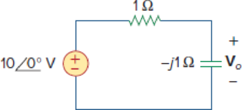
The voltage Vo across the capacitor in Fig. 10.43 is:


Figure 10.43
For Review Question 10.1.
Choose the correct option to find the voltage
Answer to Problem 1RQ
The correct option from the given choices is
Explanation of Solution
Given data:
Refer to Figure 10.43 in the textbook for circuit analysis.
Calculation:
From Figure 10.43, write the expression for voltage
Reduce the equation as follows.
Hence, the voltage across the capacitor is
Conclusion:
Thus, the correct option from the given choices is
Want to see more full solutions like this?
Chapter 10 Solutions
EBK FUNDAMENTALS OF ELECTRIC CIRCUITS
Additional Engineering Textbook Solutions
Starting Out with Java: From Control Structures through Objects (7th Edition) (What's New in Computer Science)
Vector Mechanics for Engineers: Statics and Dynamics
Fluid Mechanics: Fundamentals and Applications
SURVEY OF OPERATING SYSTEMS
Java: An Introduction to Problem Solving and Programming (8th Edition)
Thinking Like an Engineer: An Active Learning Approach (4th Edition)


- A certain signal f(t) has the following PSD (assume 12 load): Sp (w) = new + 8(w) - 1.5) + (w + 1.5)] (a) What is the mean power in the bandwidth w≤2 rad/see? (b) What is the mean power in the bandwidth -1.9 to 0.99 rad/sec? Paress(w) dw 2ㅈ -arrow_forward(75 Marks) JA signal (t) is bond 7)(t)(t) and f(t), are band-limited to 1.2 kHz each. These signals are to be limited to 9.6 kHz, and three other signals transmitted by means of time-division multiplexing. Set up scheme for accomplishing this multiplexing requirement, with each signal sampled at its Nyquist rate. What must be the speed of the commutator (the output but ram-k bit/sec)? the minimum band width? (25 Marks)arrow_forwardDraw the digital modulation outputs, ASK Amplitude Shift Keying) FSK (Frequency Shift Keying) and PSK (Phase Shift Keying). For baseband and carriet frequency as shown 101 wwwwwwwwwwww 010 BASESAND basband CARRIER Carralarrow_forward
- please show full working. I've included the solutionarrow_forwardcan you please show working and steps. The answer is 8kohms.arrow_forwardPSD A certain signal f(t) has the following PSD (assume 12 load): | Sƒ(w) = π[e¯\w\ + 8(w − 2) + +8(w + 2)] (a) What is the mean power in the bandwidth w≤ 1 rad/sec? (b) What is the mean power in the bandwidth 0.99 to 1.01 rad/sec? (c) What is the mean power in the bandwidth 1.99 to 2.01 rad/sec? (d) What is the total mean power in (t)? Pav= + 2T SfLw) dw - SALW)arrow_forward
- An AM modulation waveform signal:- p(t)=(8+4 cos 1000πt + 4 cos 2000πt) cos 10000nt (a) Sketch the amplitude spectrum of p(t). (b) Find total power, sideband power and power efficiency. (c) Find the average power containing of each sideband.arrow_forwardCan you rewrite the solution because it is unclear? AM (+) = 8(1+ 0.5 cos 1000kt +0.5 ros 2000ks) = cos 10000 πt. 8 cos wat + 4 cos wit + 4 cos Wat coswet. -Jet jooort J11000 t = 4 e jqooort jgoort +4e + e +e j 12000rt. 12000 kt + e +e jooxt igoo t te (w) = 8ES(W- 100007) + 8IS (W-10000) USBarrow_forwardCan you rewrite the solution because it is unclear? AM (+) = 8(1+0.5 cos 1000kt +0.5 ros 2000 thts) = cos 10000 πt. 8 cos wat + 4 cos wit + 4 cos Wat coswet. J4000 t j11000rt $14+) = 45 jqooort +4e + e + e j 12000rt. 12000 kt + e +e +e Le jsoort -; goon t te +e Dcw> = 885(W- 100007) + 8 IS (W-10000) - USBarrow_forward
- Can you rewrite the solution because it is unclear? Q2 AM ①(+) = 8 (1+0.5 cos 1000πt +0.5 ros 2000kt) $4+) = 45 = *cos 10000 πt. 8 cos wat + 4 cosat + 4 cos Wat coswet. j1000016 +4e -j10000πt j11000Rt j gooort -j 9000 πt + e +e j sooort te +e J11000 t + e te j 12000rt. -J12000 kt + с = 8th S(W- 100007) + 8 IS (W-10000) <&(w) = USB -5-5 -4-5-4 b) Pc 2² = 64 PSB = 42 + 4 2 Pt Pc+ PSB = y = Pe c) Puss = PLSB = = 32 4² = 8 w 32+ 8 = × 100% = 140 (1)³×2×2 31 = 20% x 2 = 3w 302 USB 4.5 5 5.6 6 ms Ac = 4 mi = 0.5 mz Ac = 4 ५ M2 = =0.5arrow_forwardA. Draw the waveform for the following binary sequence using Bipolar RZ, Bipolar NRZ, and Manchester code. Data sequence= (00110100) B. In a binary PCM system, the output signal-to-quantization ratio is to be hold to a minimum of 50 dB. If the message is a single tone with fm-5 kHz. Determine: 1) The number of required levels, and the corresponding output signal-to-quantizing noise ratio. 2) Minimum required system bandwidth.arrow_forwardFind Io using Mesh analysisarrow_forward
 Introductory Circuit Analysis (13th Edition)Electrical EngineeringISBN:9780133923605Author:Robert L. BoylestadPublisher:PEARSON
 Delmar's Standard Textbook Of ElectricityElectrical EngineeringISBN:9781337900348Author:Stephen L. HermanPublisher:Cengage Learning
 Programmable Logic ControllersElectrical EngineeringISBN:9780073373843Author:Frank D. PetruzellaPublisher:McGraw-Hill Education
 Fundamentals of Electric CircuitsElectrical EngineeringISBN:9780078028229Author:Charles K Alexander, Matthew SadikuPublisher:McGraw-Hill Education
 Electric Circuits. (11th Edition)Electrical EngineeringISBN:9780134746968Author:James W. Nilsson, Susan RiedelPublisher:PEARSON
 Engineering ElectromagneticsElectrical EngineeringISBN:9780078028151Author:Hayt, William H. (william Hart), Jr, BUCK, John A.Publisher:Mcgraw-hill Education,