Concept explainers
Videos
(a)
Calculate the energy stored in each energy storage element.
(a)
Answer to Problem 70E
The value of energy stored in the inductor
Explanation of Solution
Given data:
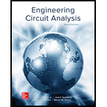
Refer to Figure 7.84 in the textbook.
Calculation:
The given circuit is redrawn as shown in Figure 1.
For a DC circuit, at steady state condition, the capacitor acts like open circuit and the inductor acts like short circuit.
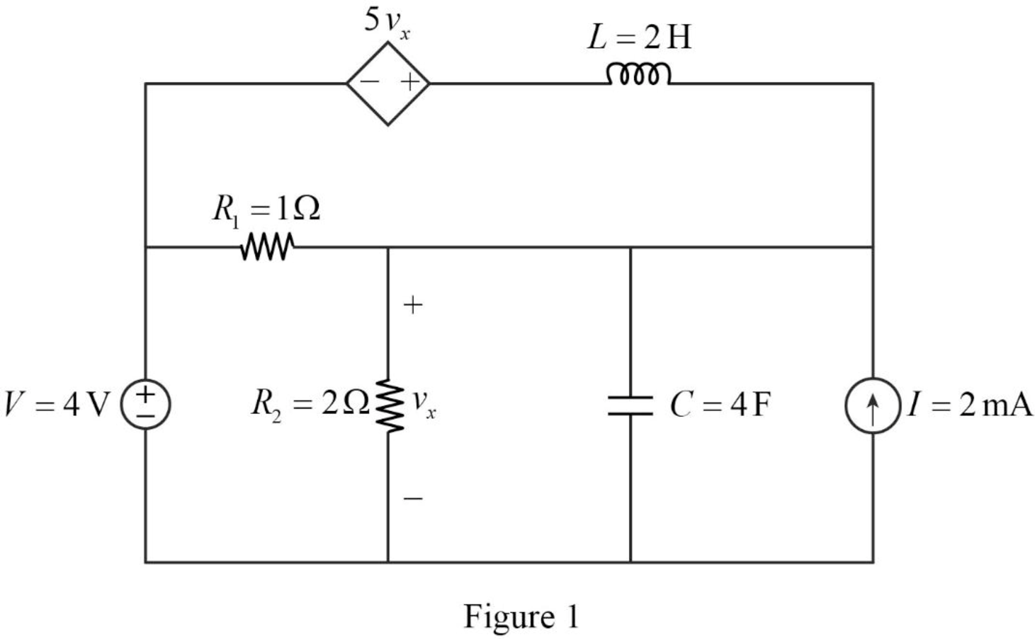
Now, the Figure 1 is reduced as shown in Figure 2.
Apply Kirchhoff’s voltage law for loop 1 in Figure 2.
Refer to Figure 2, the current
Substitute
Simplify the above equation to find
Apply Kirchhoff’s voltage law for loop 3 in Figure 2.
Refer to Figure 2, the voltage across the resistor
The voltage
Substitute equation (4) in (3).
Substitute
Substitute equation (2) in (5).
Simplify the above equation to find
Substitute
Refer to Figure 2, the current
Substitute
Refer to Figure 2, the resistor
Write a general expression to calculate the energy stored in a inductor.
Here,
Write a general expression to calculate the energy stored in a capacitor.
Here,
Substitute
Simplify the above equation to find
Substitute
Simplify the above equation to find
Conclusion:
Thus, the value of energy stored in the inductor
(b)
Verify the calculated answers with an appropriate simulation.
(b)
Explanation of Solution
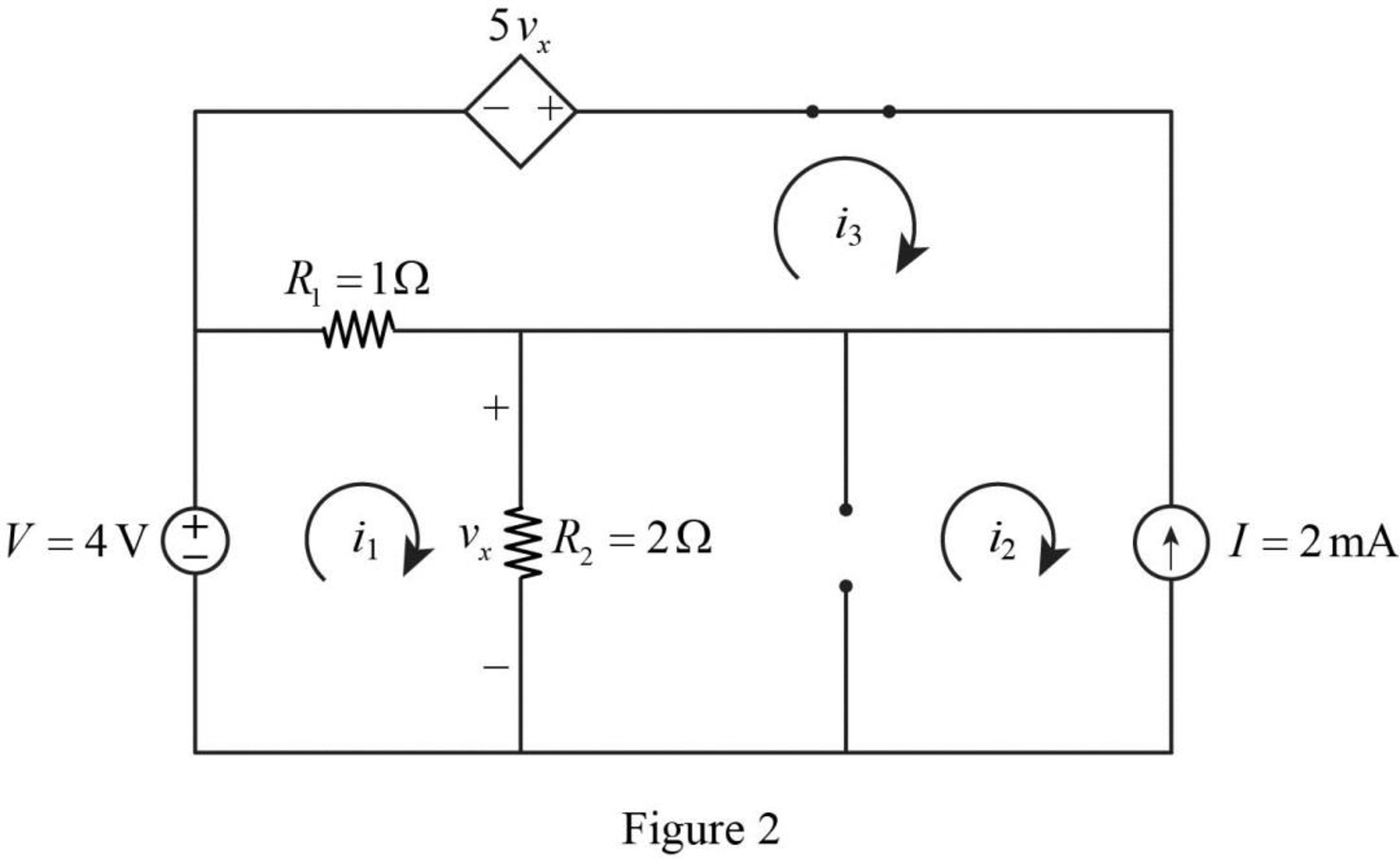
Create the new schematic in LTspice and draw the Figure 1 as shown in Figure 3. Use the Label net option and write VR2 to find voltage across resistor
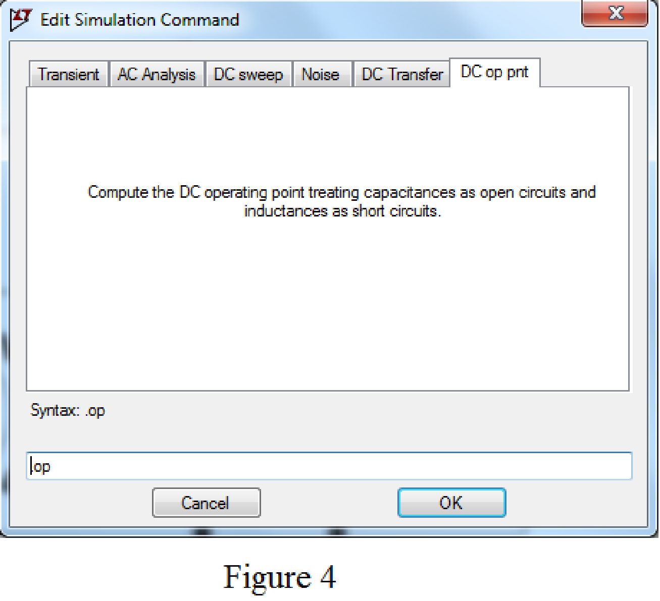
Choose the Dc op point in Edit simulation Cmd as shown in Figure 4.
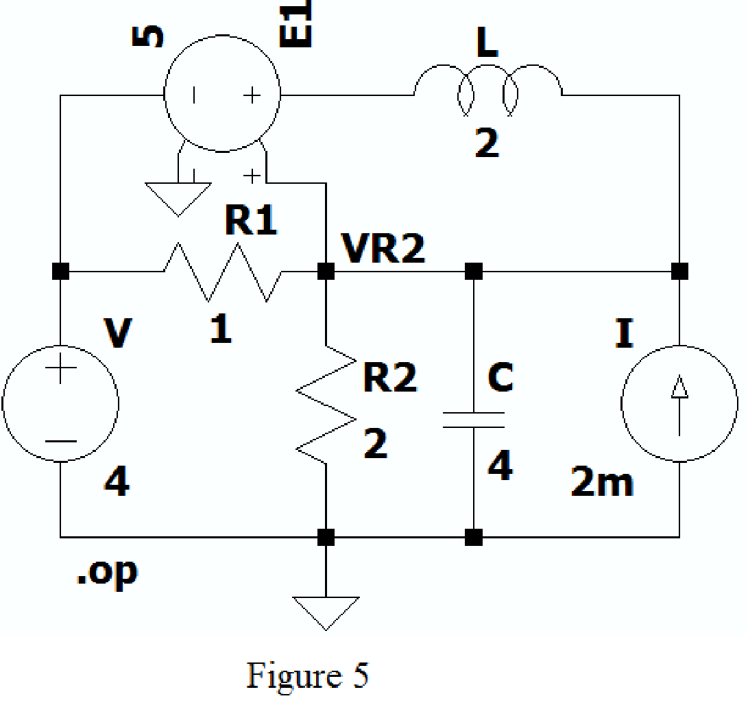
After adding the above mentioned commands the circuit becomes as shown in Figure 5.
Now run the simulation, the table will be displayed with the values of current through resistors, capacitor and voltage across the capacitor as shown in Figure 6.
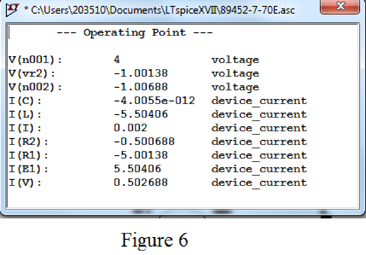
Refer to Figure 6, the value of voltage across the capacitor
Conclusion:
Thus, the calculated answers are verified with an appropriate SPICE simulation.
Want to see more full solutions like this?
Chapter 7 Solutions
Loose Leaf for Engineering Circuit Analysis Format: Loose-leaf


- Solve this problem and show all of the workarrow_forwardI need help with this problem and an step by step explanation of the solution from the image described below. (Introduction to Signals and Systems)arrow_forwardI need help with this problem and an step by step explanation of the solution from the image described below. (Introduction to Signals and Systems)arrow_forward
- I need help with this problem and an step by step explanation of the solution from the image described below. (Introduction to Signals and Systems)arrow_forwardI need help with this problem and an step by step explanation of the solution from the image described below. (Introduction to Signals and Systems)arrow_forwardI need help with this problem and an step by step explanation of the solution from the image described below. (Introduction to Signals and Systems)arrow_forward
- 2) Design the circuit shown in Figure 2 to provide bias current of IQ2= 150 uA. Assume circuit parameters of IREF2 = 250 UA, V+ = 3 V, and V = -3 V. The transistor parameters are VTP = -0.6 V, λ = 0, K'p= 40 uA/V², W/Lc = 15 and W/LA = 25. V+ Mc + VSGC VSGB + MB VSGA + + MA VSDA IREF2 V- Figure 2 ww RD=8kQarrow_forward٣/١ a い يكا +91- PU + 96852 A. For the RL-circuit with i(0)=0, Find the current i(t) using LT R=2 V(t)=sin3t L=1H B. Find Invers Laplace Transform for Z(s) = = 220125 750 x2.01 4s2 +2s+3 s2-3s+2arrow_forward1) Taking base current into account, determine the value of I copy in each circuit depicted in Fig 1. Normalize the error to nominal value of Icopy. REF Vcc AE Vcc QREF Figure 1- a I copy 5AE REF 12 Q₁ copy Q2 5AE 2AE ЗАЕ QREF Figure 1-barrow_forward
 Introductory Circuit Analysis (13th Edition)Electrical EngineeringISBN:9780133923605Author:Robert L. BoylestadPublisher:PEARSON
 Delmar's Standard Textbook Of ElectricityElectrical EngineeringISBN:9781337900348Author:Stephen L. HermanPublisher:Cengage Learning
 Programmable Logic ControllersElectrical EngineeringISBN:9780073373843Author:Frank D. PetruzellaPublisher:McGraw-Hill Education
 Fundamentals of Electric CircuitsElectrical EngineeringISBN:9780078028229Author:Charles K Alexander, Matthew SadikuPublisher:McGraw-Hill Education
 Electric Circuits. (11th Edition)Electrical EngineeringISBN:9780134746968Author:James W. Nilsson, Susan RiedelPublisher:PEARSON
 Engineering ElectromagneticsElectrical EngineeringISBN:9780078028151Author:Hayt, William H. (william Hart), Jr, BUCK, John A.Publisher:Mcgraw-hill Education,