
Concept explainers
Videos
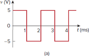
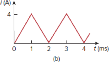
A square-wave generator produces the voltage waveform shown in Fig. 6.94(a). What kind of a circuit component is needed to convert the voltage waveform to the triangular current waveform shown in Fig. 6.94(b)? Calculate the value of the component, assuming that it is initially uncharged.
Figure 6.94
For Prob. 6.85.
Find the circuit component that is needed to convert the voltage waveform into the triangular current waveform and to calculate the value of the circuit component.
Answer to Problem 85CP
The circuit component inductor is needed to convert the given voltage waveform into the triangular current waveform and the value for the inductor
Explanation of Solution
Given data:
Refer to Figure 6.94 in the textbook.
Formula used:
Write the expression to calculate the straight line equation for two points
Refer to Figure 6.94(b) in the textbook.
From the given graph, substitute
Calculation:
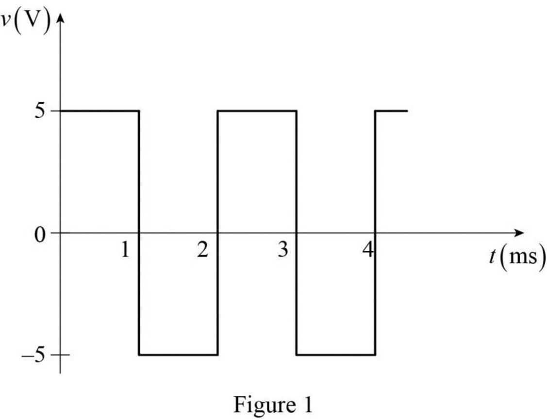
The given voltage waveform is redrawn as Figure 1.
The given triangular current waveform is redrawn as Figure 2.
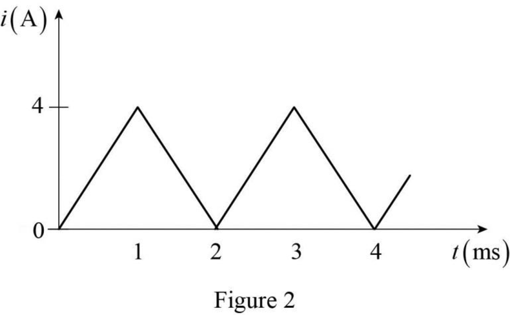
Refer to Figure 1 and Figure 2. Generally, integration of the square waveform gives the triangular waveform. That is, the integration of the voltage waveform gives the current waveform. Such relation can be obtained in following relation.
Here,
Refer to equation (3), the circuit component inductor is needed to convert the square voltage waveform to the triangular current waveform.
Differentiate the equation (3) with respect to
Rearrange the above equation to find
Refer to Figure 1. The voltage function is expressed as,
Refer to Figure 2, split up the time period as four divisions
Case (i):
The two points
Substitute
Simplify the equation to find
Case (ii):
The two points
Substitute
Simplify the equation to find
Case (iii):
The two points
Substitute
Simplify the equation to find
Case (iv):
The two points
Substitute
Simplify the equation to find
Therefore, the current function of the signal in Figure 2 is,
For
Substitute
For
Substitute
For
Substitute
For
Substitute
Therefore, the voltage function of the Figure 2 is expressed as,
The voltage function of the signal in Figure 1 is equal to the voltage function that is obtained in equation (6).
Compare the equations (5) and (6) for any of the time limits. Assume the comparison is made for
Rearrange the above equation to find
Therefore, the circuit component inductor is needed to convert the given voltage waveform into the triangular current waveform and the value for the inductor
Conclusion:
Thus, the circuit component inductor is needed to convert the given voltage waveform into the triangular current waveform and the value for the inductor
Want to see more full solutions like this?
Chapter 6 Solutions
EBK FUNDAMENTALS OF ELECTRIC CIRCUITS


- : Write VHDL code to implement the finite-state machine/described by the state Diagram in Fig. 4. X=1 X=0 solo X=1 X=0 $1/1 X=0 X=1 X=1 52/2 $3/3 X=1 Fig. 4 X=1 X=1 56/6 $5/5 X=1 54/4 X=0 X-O X=O 5=0 57/7arrow_forwardQuestions: Q1: Verify that the average power generated equals the average power absorbed using the simulated values in Table 7-2. Q2: Verify that the reactive power generated equals the reactive power absorbed using the simulated values in Table 7-2. Q3: Why it is important to correct the power factor of a load? Q4: Find the ideal value of the capacitor theoretically that will result in unity power factor. Vs pp (V) VRIPP (V) VRLC PP (V) AT (μs) T (us) 8° pf Simulated 14 8.523 7.84 84.850 1000 29.88 0.866 Measured 14 8.523 7.854 82.94 1000 29.85 0.86733 Table 7-2 Power Calculations Pvs (mW) Qvs (mVAR) PRI (MW) Pay (mW) Qt (mVAR) Qc (mYAR) Simulated -12.93 -7.428 9.081 3.855 12.27 -4.84 Calculated -12.936 -7.434 9.083 3.856 12.32 -4.85 Part II: Power Factor Correction Table 7-3 Power Factor Correction AT (us) 0° pf Simulated 0 0 1 Measured 0 0 1arrow_forwardQuestions: Q1: Verify that the average power generated equals the average power absorbed using the simulated values in Table 7-2. Q2: Verify that the reactive power generated equals the reactive power absorbed using the simulated values in Table 7-2. Q3: Why it is important to correct the power factor of a load? Q4: Find the ideal value of the capacitor theoretically that will result in unity power factor. Vs pp (V) VRIPP (V) VRLC PP (V) AT (μs) T (us) 8° pf Simulated 14 8.523 7.84 84.850 1000 29.88 0.866 Measured 14 8.523 7.854 82.94 1000 29.85 0.86733 Table 7-2 Power Calculations Pvs (mW) Qvs (mVAR) PRI (MW) Pay (mW) Qt (mVAR) Qc (mYAR) Simulated -12.93 -7.428 9.081 3.855 12.27 -4.84 Calculated -12.936 -7.434 9.083 3.856 12.32 -4.85 Part II: Power Factor Correction Table 7-3 Power Factor Correction AT (us) 0° pf Simulated 0 0 1 Measured 0 0 1arrow_forward
- electric plants. Prepare the load schedulearrow_forwardelectric plants Draw the column diagram. Calculate the voltage drop. by hand writingarrow_forwardelectric plants. Draw the lighting, socket, telephone, TV, and doorbell installations on the given single-story project with an architectural plan by hand writingarrow_forward
- A circularly polarized wave, traveling in the +z-direction, is received by an elliptically polarized antenna whose reception characteristics near the main lobe are given approx- imately by E„ = [2â, + jâ‚]ƒ(r. 8, 4) Find the polarization loss factor PLF (dimensionless and in dB) when the incident wave is (a) right-hand (CW) An elliptically polarized wave traveling in the negative z-direction is received by a circularly polarized antenna. The vector describing the polarization of the incident wave is given by Ei= 2ax + jay.Find the polarization loss factor PLF (dimensionless and in dB) when the wave that would be transmitted by the antenna is (a) right-hand CParrow_forwardjX(1)=j0.2p.u. jXa(2)=j0.15p.u. jxa(0)=0.15 p.u. V₁=1/0°p.u. V₂=1/0° p.u. 1 jXr(1) = j0.15 p.11. jXT(2) = j0.15 p.u. jXr(0) = j0.15 p.u. V3=1/0° p.u. А V4=1/0° p.u. 2 jX1(1)=j0.12 p.u. 3 jX2(1)=j0.15 p.u. 4 jX1(2)=0.12 p.11. JX1(0)=0.3 p.u. jX/2(2)=j0.15 p.11. X2(0)=/0.25 p.1. Figure 1. Circuit for Q3 b).arrow_forwardcan you show me full workings for this problem. the solution is - v0 = 10i2 = 2.941 volts, i0 = i1 – i2 = (5/3)i2 = 490.2mA.arrow_forward
- Q4. a) Consider a transmission line modelled as a four-terminal network with an unknown configuration. You are provided with the following measured parameters at the operating frequency: Open-circuit voltage ratio: 0.9521° • Short-circuit impedance: 40+j80 • Open-circuit admittance: -j2 × 10-4 S Use the four terminal equations and the provided measurements to mathematically derive the A, B, C, and D parameters of the network and explain their physical significance. Show your work and formulas used in the derivation.arrow_forwardQ1. Consider a single-phase step-down transformer with primary and secondary turns of 600 and 100 respectively and a primary voltage of 11 kV. (i) An open circuit test was conducted on the transformer and the primary current was measured as: I₁ = 2.20 A Use these results to calculate the magnetising reactance in the equivalent circuit (X) given that Rm, representing the core loss, has a value of 21 km. (ii) The remaining equivalent circuit parameters are as follows: R₁ = 40, X₁ = 25 N, R₂ = 0.4 N, X₂ = 0.3 N Draw the complete simplified equivalent circuit, by referring series components on the primary side to the secondary, giving all component values. (iii) The transformer is connected, on its secondary side, to a load of 10 at a power factor of 1. Calculate the voltage across the load. (iv) Calculate the efficiency of the transformer when operating at the load given in part (iii).arrow_forwardb) A 132 kV supply feeds a line of reactance 15 which is connected to a 100 MVA, 132/33 kV transformer of 0.08 p.u. reactance as shown in the Figure 2. The transformer feeds a 33 kV line of reactance 8 Q, which, in turn, is connected to a 75 MVA, 33/11 KV transformer of 0.12 p.u. reactance. The transformer supplies an 11 KV substation from which a local 11 kV feeder of 4 Q reactance is supplied. T1 T2 132 kV 33 kV 11 kV Fault X CB Relay Figure 2. Network for Q4 b). (i) Given the system base of 100 MVA, compute the total equivalent reactance of the radial circuit in per unit (p.u.). (ii) Determine the three-phase fault current at the load end of the 11 kV feeder, assuming a fault impedance of 0.05 Q. Calculate the fault current in Amperes. (iii) The 11 kV feeder connects to a protective overcurrent relay via 200/5 A current transformers. This relay has a standard normally inverse IDMT characteristic, with a setting current of 3 A and a time multiplier setting of 0.4. Calculate the…arrow_forward
 Delmar's Standard Textbook Of ElectricityElectrical EngineeringISBN:9781337900348Author:Stephen L. HermanPublisher:Cengage Learning