
MICROELECT. CIRCUIT ANALYSIS&DESIGN (LL)
4th Edition
ISBN: 9781266368622
Author: NEAMEN
Publisher: MCG
expand_more
expand_more
format_list_bulleted
Videos
Textbook Question
Chapter 5, Problem 5.39P
Let
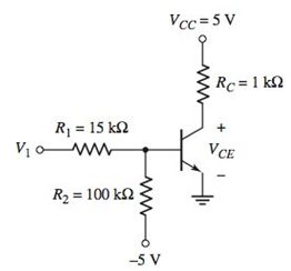
Figure P5.39
Expert Solution & Answer
Want to see the full answer?
Check out a sample textbook solution
Students have asked these similar questions
electric plants
do hand writing
please solve quickly. thank you!
Please show all steps
Chapter 5 Solutions
MICROELECT. CIRCUIT ANALYSIS&DESIGN (LL)
Ch. 5 - An npn transistor is biased in the forwardactive...Ch. 5 - (a) The common-emitter current gains of two...Ch. 5 - An npn transistor is biased in the forwardactive...Ch. 5 - The emitter current in a pnp transistor biased in...Ch. 5 - The output resistance of a bipolar transistor is...Ch. 5 - Assume that IC=1mA at VCE=1V , and that VBE is...Ch. 5 - The openemitter breakdown voltage is BVCBO=200V ,...Ch. 5 - A particular transistor circuit requires a minimum...Ch. 5 - The circuit elements in Figure 5.20(a) are changed...Ch. 5 - The circuit elements in Figure 5.22(a) are V+=3.3V...
Ch. 5 - (a) Verify the results of Example 5.3 with a...Ch. 5 - Consider the pnp circuit in Figure 5.22(a). Assume...Ch. 5 - In the following exercise problems, assume...Ch. 5 - In the following exercise problems, assume...Ch. 5 - The circuit elements in Figure 5.27(a) are changed...Ch. 5 - Using a PSpice simulation, plot the voltage...Ch. 5 - The parameters of the circuit shown in Figure...Ch. 5 - Design the commonbase circuit shown in Figure 5.33...Ch. 5 - The bias voltages in the circuit shown in Figure...Ch. 5 - The bias voltages in the circuit shown in Figure...Ch. 5 - The circuit elements in Figure 5.36(a) are V+=5V ,...Ch. 5 - For the transistor shown in the circuit of Figure...Ch. 5 - For the circuit shown in Figure 5.41, determine...Ch. 5 - Assume =120 for the transistor in Figure 5.42....Ch. 5 - For the transistor in Figure 5.43, assume =90 ....Ch. 5 - (a) Redesign the LED circuit in Figure 5.45(a)...Ch. 5 - The transistor parameters in the circuit in Figure...Ch. 5 - Redesign the inverter amplifier circuit shown in...Ch. 5 - For the circuit shown in Figure 5.44, assume...Ch. 5 - Consider the circuit shown in Figure 5.51(b)....Ch. 5 - [Note: In the following exercises, assume the BE...Ch. 5 - [Note: In the following exercises, assume the B—E...Ch. 5 - Consider the circuit in Figure 5.54(a), let...Ch. 5 - Prob. 5.16EPCh. 5 - The parameters of the circuit shown in Figure...Ch. 5 - Consider the circuit in Figure 5.54(a). The...Ch. 5 - Consider the circuit shown in Figure 5.58. The...Ch. 5 - In the circuit shown in Figure 5.60, the...Ch. 5 - The parameters of the circuit shown in Figure...Ch. 5 - For Figure 5.59, the circuit parameters are...Ch. 5 - In the circuit shown in Figure 5.61, determine new...Ch. 5 - For the circuit shown in Figure 5.63, the circuit...Ch. 5 - (a) Verily the cascode circuit design in Example...Ch. 5 - Prob. 1RQCh. 5 - Prob. 2RQCh. 5 - Prob. 3RQCh. 5 - Define commonbase current gain and commonemitter...Ch. 5 - Discuss the difference between the ac and dc...Ch. 5 - State the relationships between collector,...Ch. 5 - Define Early voltage and collector output...Ch. 5 - Describe a simple commonemitter circuit with an...Ch. 5 - Prob. 9RQCh. 5 - Prob. 10RQCh. 5 - Prob. 11RQCh. 5 - Describe a bipolar transistor NOR logic circuit.Ch. 5 - Describe how a transistor can be used to amplify a...Ch. 5 - Discuss the advantages of using resistor voltage...Ch. 5 - Prob. 15RQCh. 5 - Prob. 16RQCh. 5 - (a) In a bipolar transistor biased in the...Ch. 5 - (a) A bipolar transistor is biased in the...Ch. 5 - (a) The range of ( for a particular type of...Ch. 5 - (a) A bipolar transistor is biased in the...Ch. 5 - Prob. 5.5PCh. 5 - An npn transistor with =80 is connected in a...Ch. 5 - Prob. 5.7PCh. 5 - A pnp transistor with =60 is connected in a...Ch. 5 - (a) The pnp transistor shown in Figure P5.8 has a...Ch. 5 - An npn transistor has a reverse-saturation current...Ch. 5 - Two pnp transistors, fabricated with the same...Ch. 5 - The collector currents in two transistors, A and...Ch. 5 - Prob. 5.13PCh. 5 - Prob. 5.14PCh. 5 - In a particular circuit application, the minimum...Ch. 5 - A particular transistor circuit design requires a...Ch. 5 - For all the transistors in Figure P5.17, =75 . The...Ch. 5 - The emitter resistor values in the circuits show...Ch. 5 - Consider the two circuits in Figure P5.19. The...Ch. 5 - The current gain for each transistor in the...Ch. 5 - Consider the circuits in Figure P5.21. For each...Ch. 5 - (a) The circuit and transistor parameters for the...Ch. 5 - In the circuits shown in Figure P5.23, the values...Ch. 5 - (a) For the circuit in Figure P5.24, determine VB...Ch. 5 - (a) The bias voltages in the circuit shown in...Ch. 5 - The transistor shown in Figure P5.26 has =120 ....Ch. 5 - The transistor in the circuit shown in Figure...Ch. 5 - In the circuit in Figure P5.27, the constant...Ch. 5 - For the circuit shown in Figure P5.29, if =200 for...Ch. 5 - The circuit shown in Figure P5.30 is to be...Ch. 5 - (a) The bias voltage in the circuit in Figure P5.3...Ch. 5 - The current gain of the transistor in the circuit...Ch. 5 - (a) The current gain of the transistor in Figure...Ch. 5 - (a) The transistor shown in Figure P5.34 has =100...Ch. 5 - Assume =120 for the transistor in the circuit...Ch. 5 - For the circuit shown in Figure P5.27, calculate...Ch. 5 - Consider the commonbase circuit shown in Figure...Ch. 5 - (a) For the transistor in Figure P5.38, =80 ....Ch. 5 - Let =25 for the transistor in the circuit shown in...Ch. 5 - (a) The circuit shown in Figure P5.40 is to be...Ch. 5 - The circuit shown in Figure P5.41 is sometimes...Ch. 5 - The transistor in Figure P5.42 has =120 . (a)...Ch. 5 - The commonemitter current gain of the transistor...Ch. 5 - For the circuit shown in Figure P5.44, plot the...Ch. 5 - The transistor in the circuit shown in Figure...Ch. 5 - Consider the circuit in Figure P5.46. For the...Ch. 5 - The current gain for the transistor in the circuit...Ch. 5 - Consider the amplifier circuit shown in Figure...Ch. 5 - For the transistor in the circuit shown in Figure...Ch. 5 - Reconsider Figure P5.49. The transistor current...Ch. 5 - The current gain of the transistor shown in the...Ch. 5 - For the circuit shown in Figure P5.52, let =125 ....Ch. 5 - Consider the circuit shown in Figure P5.53. (a)...Ch. 5 - (a) Redesign the circuit shown in Figure P5.49...Ch. 5 - Prob. 5.55PCh. 5 - Consider the circuit shown in Figure P5.56. (a)...Ch. 5 - (a) Determine the Q-point values for the circuit...Ch. 5 - (a) Determine the Q-point values for the circuit...Ch. 5 - (a) For the circuit shown in Figure P5.59, design...Ch. 5 - Design a bias-stable circuit in the form of Figure...Ch. 5 - Using the circuit in Figure P5.61, design a...Ch. 5 - For the circuit shown in Figure P5.61, the bias...Ch. 5 - (a) A bias-stable circuit with the configuration...Ch. 5 - (a) For the circuit shown in Figure P5.64, assume...Ch. 5 - The dc load line and Q-point of the circuit in...Ch. 5 - The range of ß for the transistor in the circuit...Ch. 5 - The nominal Q-point of the circuit in Figure P5.67...Ch. 5 - (a) For the circuit in Figure P5.67, the value of...Ch. 5 - For the circuit in Figure P5.69, let =100 and...Ch. 5 - Prob. 5.70PCh. 5 - Design the circuit in Figure P5.70 to be bias...Ch. 5 - Consider the circuit shown in Figure P5.72. (a)...Ch. 5 - For the circuit in Figure P5.73, let =100 . (a)...Ch. 5 - Prob. D5.74PCh. 5 - (a) Design a fourresistor bias network with the...Ch. 5 - (a) Design a four-resistor bias network with the...Ch. 5 - (a) A fourresistor bias network is to be designed...Ch. 5 - (a) Design a fourresistor bias network with the...Ch. 5 - For each transistor in the circuit in Figure...Ch. 5 - The parameters for each transistor in the circuit...Ch. 5 - The bias voltage in the circuit shown in Figure...Ch. 5 - Consider the circuit shown in Figure P5.82. The...Ch. 5 - (a) For the transistors in the circuit shown in...Ch. 5 - Using a computer simulation, plot VCE versus V1...Ch. 5 - Using a computer simulation, verify the results of...Ch. 5 - Using a computer simulation, verify the results of...Ch. 5 - Consider a commonemitter circuit with the...Ch. 5 - The emitterfollower circuit shown in Figure P5.89...Ch. 5 - The bias voltages for the circuit in Figure...Ch. 5 - The multitransistor circuit in Figure 5.61 is to...
Knowledge Booster


Learn more about
Need a deep-dive on the concept behind this application? Look no further. Learn more about this topic, electrical-engineering and related others by exploring similar questions and additional content below.Similar questions
- 12-3) PDF, mean, & variance A random variable has the PDF shown in the figure. a) Find the numerical value of the parameter K. b) Write the numerical expression for the PDF. c) Find the probability that the random variable is negative. d) Find the mean of x, the expected value of x², and the variance of x. K Px(x) 3 Xarrow_forwardPlease show all stepsarrow_forward12-4) Gaussian random variable A Gaussian random variable has a mean value of 4 and a standard deviation of 3. Find the probability that the value of the random variable exceeds 16. Repeat for the probability that it is less than -2. The discussion of Marcum's Q function given in the lecture notes may be helpful.arrow_forward
- A transformer has a primary voltage of 240 V and a secondary voltage of 48 V. What is the turns ratio of this transformer?arrow_forwardmicroprocers and microcontrolerarrow_forwardDesign a counter to count-up from 2 to 7 using three of D Flip Flops (3) 3-Bit Count up (3 to 5) Using D Flip-Flop: The State Equation of D Flip-Flop: Q(t+1)=D(t) => Dn=Qn Present State D Flip-Flop Next State n Q2p Q1p Q0p 3 0 1 1 1 Q2n Q1n Q0n D2 D1 D0 0 0 1 0 0 4 1 0 0 1 0 1 1 0 1 5 1 0 1 0 1 1 01 1 D2-Sum(3,4) and don't care X-Sum(0,1,2,6,7) D1=Sum(5) and don't care X=Sum(0,1,2,6,7) D0=Sum(4,5) and don't care X=Sum(0,1,2,6,7) Using K-map to simplify the functions: D2=Q1+Q0' D1=Q1'QO DO=Q1' XOX XOX Q2 10 Q2 01 Q2 1xx Q0 QO Qo D2 Q2 >CK Q2 D1 Q1 BCD CK Q1 DO QF ►CK Q0 ☐ Present State Next State D Flip-Flop n Q2p Q1p Q0p Q2n Q1n Q0n D2 D1 D0 2 0 1 0 0 1 1 0 1 1 3 0 1 1 1 0 0 1 00 4 1 0 0 1 0 1 1 0 1 5 1 0 1 1 1 0 1 1 0 6 1 1 0 0 1 0 0 1 0 D2 D2=Sum(3,4,5), X=Sum(0,1,7) D1 Q2 1 Q1 1 0 ☑ 0 Qo D2=Q0+Q1' ✗ 0 Q1arrow_forward
- Consider the following 4×1 multiplexer with inputs: w0=2, w1=1, w2=x2' and w3=0 And with switches: S1 x1 and S0=x0 What is the multiplexer output f as a function of x2, x1 and x0?arrow_forwardI need help adding a capacitor and a Zener diode to my circuit. I’m looking for a simple sketch or diagram showing how to connect them. i want diagram with final circuit after adding the zener diad and capacitor. don't do calclution or anything. thanksarrow_forwardQuestion 3 AC Motor Drives [15]Calculate the instantaneous currents delivered by the inverter if the direct axiscurrent required at a particular instant is 8.66A and the quadrature current is5A. Derive all equations for the three currents.arrow_forward
- A certain signal f(t) has the following PSD (assume 12 load): Sp (w) = new + 8(w) - 1.5) + (w + 1.5)] (a) What is the mean power in the bandwidth w≤2 rad/see? (b) What is the mean power in the bandwidth -1.9 to 0.99 rad/sec? Paress(w) dw 2ㅈ -arrow_forward(75 Marks) JA signal (t) is bond 7)(t)(t) and f(t), are band-limited to 1.2 kHz each. These signals are to be limited to 9.6 kHz, and three other signals transmitted by means of time-division multiplexing. Set up scheme for accomplishing this multiplexing requirement, with each signal sampled at its Nyquist rate. What must be the speed of the commutator (the output but ram-k bit/sec)? the minimum band width? (25 Marks)arrow_forwardDraw the digital modulation outputs, ASK Amplitude Shift Keying) FSK (Frequency Shift Keying) and PSK (Phase Shift Keying). For baseband and carriet frequency as shown 101 wwwwwwwwwwww 010 BASESAND basband CARRIER Carralarrow_forward
arrow_back_ios
SEE MORE QUESTIONS
arrow_forward_ios
Recommended textbooks for you
 Introductory Circuit Analysis (13th Edition)Electrical EngineeringISBN:9780133923605Author:Robert L. BoylestadPublisher:PEARSON
 Delmar's Standard Textbook Of ElectricityElectrical EngineeringISBN:9781337900348Author:Stephen L. HermanPublisher:Cengage Learning
 Programmable Logic ControllersElectrical EngineeringISBN:9780073373843Author:Frank D. PetruzellaPublisher:McGraw-Hill Education
 Fundamentals of Electric CircuitsElectrical EngineeringISBN:9780078028229Author:Charles K Alexander, Matthew SadikuPublisher:McGraw-Hill Education
 Electric Circuits. (11th Edition)Electrical EngineeringISBN:9780134746968Author:James W. Nilsson, Susan RiedelPublisher:PEARSON
 Engineering ElectromagneticsElectrical EngineeringISBN:9780078028151Author:Hayt, William H. (william Hart), Jr, BUCK, John A.Publisher:Mcgraw-hill Education,
Introductory Circuit Analysis (13th Edition)
Electrical Engineering
ISBN:9780133923605
Author:Robert L. Boylestad
Publisher:PEARSON
Delmar's Standard Textbook Of Electricity
Electrical Engineering
ISBN:9781337900348
Author:Stephen L. Herman
Publisher:Cengage Learning
Programmable Logic Controllers
Electrical Engineering
ISBN:9780073373843
Author:Frank D. Petruzella
Publisher:McGraw-Hill Education
Fundamentals of Electric Circuits
Electrical Engineering
ISBN:9780078028229
Author:Charles K Alexander, Matthew Sadiku
Publisher:McGraw-Hill Education
Electric Circuits. (11th Edition)
Electrical Engineering
ISBN:9780134746968
Author:James W. Nilsson, Susan Riedel
Publisher:PEARSON
Engineering Electromagnetics
Electrical Engineering
ISBN:9780078028151
Author:Hayt, William H. (william Hart), Jr, BUCK, John A.
Publisher:Mcgraw-hill Education,
How a MOSFET Works - with animation! | Intermediate Electronics; Author: CircuitBread;https://www.youtube.com/watch?v=Bfvyj88Hs_o;License: Standard Youtube License