
EBK COMPUTER SCIENCE ILLUMINATED
7th Edition
ISBN: 9781284174755
Author: Dale
Publisher: JONES+B CO
expand_more
expand_more
format_list_bulleted
Videos
Question
Chapter 4, Problem 62E
Program Plan Intro
Circuit:
- The circuit is known as the combination of gates that is used to achieve a difficult logical operation.
- It has two general categories, they are:
- Combinational circuit
- Sequential circuit
Expert Solution & Answer
Explanation of Solution
Given circuit:
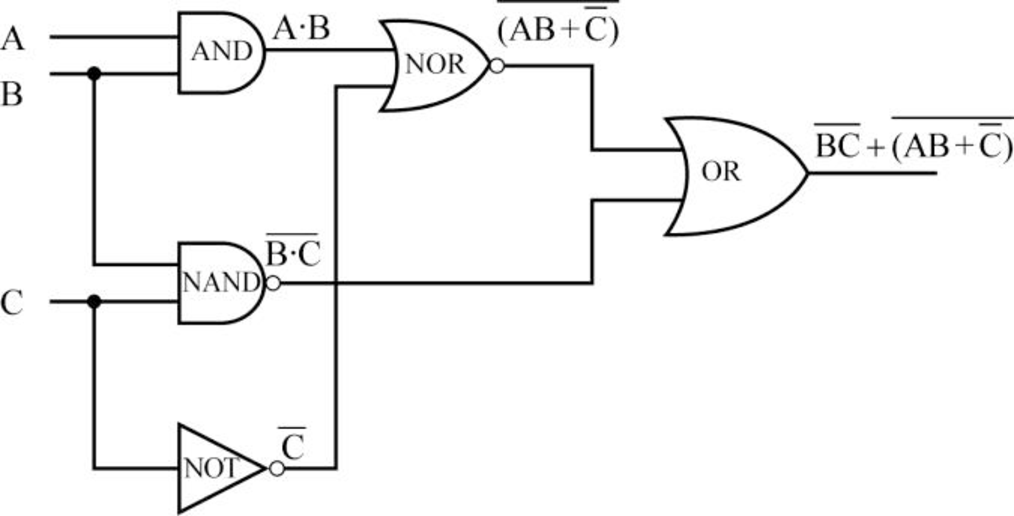
Behavior of the circuit:
- From the above circuit diagram,
- First, the inputs A and B are passed to AND gate to perform the product of A and B and produce the output as
- Next, pass the same input B from the AND gate, and input C is passed in the NAND gate to perform the inverse of product of B and C and produce the output as
- Next, pass the same input C from the NAND gate to NOT gate, to perform the inverse of C to produce the output as
- Next, pass the output of AND gate and output of NOT gate as the input to NOR gate to perform the inverse of sum of “
- Finally, the output of NOR gate and output of NAND gate is passed as the input of OR gate.
- Therefore, “
- Therefore, “
- First, the inputs A and B are passed to AND gate to perform the product of A and B and produce the output as
Truth table for the above circuit diagram:
Step 1:
- The inputs are A, B, and C for the circuit diagram:
| A | B | C | |||||
| 0 | 0 | 0 | |||||
| 0 | 0 | 1 | |||||
| 0 | 1 | 0 | |||||
| 0 | 1 | 1 | |||||
| 1 | 0 | 0 | |||||
| 1 | 0 | 1 | |||||
| 1 | 1 | 0 | |||||
| 1 | 1 | 1 |
Step 2:
- When the inputs are A as 0, B as 0, and C as 0:
| A | B | C | |||||
| 0 | 0 | 0 | 0 | 1 | 1 | 0 | 1 |
| 0 | 0 | 1 | |||||
| 0 | 1 | 0 | |||||
| 0 | 1 | 1 | |||||
| 1 | 0 | 0 | |||||
| 1 | 0 | 1 | |||||
| 1 | 1 | 0 | |||||
| 1 | 1 | 1 |
- First, the inputs A as 0 and B as 0 are passed to AND gate to perform the product of 0 and 0 and produce the output as
- Next, pass the same input B as 0 from the AND gate
- Next, pass the same input C as 0 from the NAND gate
- Next, pass the output of AND gate and output of NOT gate as the input for NOR gate to perform the inverse of sum of “0” and “1”, and produce the output as
- Finally, the output of NOR gate and output of NAND gate is passed as the input of OR gate.
- Therefore, “0” and “1” are passed as input to OR gate and produce the output as
- Therefore, “0” and “1” are passed as input to OR gate and produce the output as
Step 3:
- When the inputs are A as 0, B as 0, and C as 1:
| A | B | C | |||||
| 0 | 0 | 0 | 0 | 1 | 1 | 0 | 1 |
| 0 | 0 | 1 | 0 | 1 | 0 | 1 | 1 |
| 0 | 1 | 0 | |||||
| 0 | 1 | 1 | |||||
| 1 | 0 | 0 | |||||
| 1 | 0 | 1 | |||||
| 1 | 1 | 0 | |||||
| 1 | 1 | 1 |
- First, the inputs A as 0 and B as 0 are passed to AND gate to perform the product of 0 and 0 and produce the output as
- Next, pass the same input B as 0 from the AND gate
- Next, pass the same input C as 1 from the NAND gate
- Next, pass the output of AND gate and output of NOT gate as the input for NOR gate to perform the inverse of sum of “0” and “0” and produces the output as
- Finally, the output of NOR gate and output of NAND gate is passed as the input of OR gate.
- Therefore, “1” and “1” are passed as input to OR gate and produce the output as
- Therefore, “1” and “1” are passed as input to OR gate and produce the output as
Step 4:
- When the inputs are A as 0, B as 1, and C as 0:
| A | B | C | |||||
| 0 | 0 | 0 | 0 | 1 | 1 | 0 | 1 |
| 0 | 0 | 1 | 0 | 1 | 0 | 1 | 1 |
| 0 | 1 | 0 | 0 | 1 | 1 | 0 | 1 |
| 0 | 1 | 1 | |||||
| 1 | 0 | 0 | |||||
| 1 | 0 | 1 | |||||
| 1 | 1 | 0 | |||||
| 1 | 1 | 1 |
- First, the inputs A as 0 and B as 1 are passed to AND gate to perform the product of 0 and 1 and produce the output as
- Next, pass the same input B as 1 from the AND gate
- Next, pass the same input C as 0 from the NAND gate
- Next, pass the output of AND gate and output of NOT gate as the input for NOR gate to perform the inverse of sum of “0” and “1” and produces the output as
- Finally, the output of NOR gate and output of NAND gate are passed as the input of OR gate.
- Therefore, “0” and “1” are passed as input to OR gate and produce the output as
- Therefore, “0” and “1” are passed as input to OR gate and produce the output as
Step 5:
- When the inputs are A as 0, B as 1, and C as 1:
| A | B | C | |||||
| 0 | 0 | 0 | 0 | 1 | 1 | 0 | 1 |
| 0 | 0 | 1 | 0 | 1 | 0 | 1 | 1 |
| 0 | 1 | 0 | 0 | 1 | 1 | 0 | 1 |
| 0 | 1 | 1 | 0 | 0 | 0 | 1 | 1 |
| 1 | 0 | 0 | |||||
| 1 | 0 | 1 | |||||
| 1 | 1 | 0 | |||||
| 1 | 1 | 1 |
- First, the inputs A as 0 and B as 1 are passed to AND gate to perform the product of 0 and 1 and produce the output as
- Next, pass the same input B as 1 from the AND gate
- Next, pass the same input C as 1 from the NAND gate
- Next, pass the output of AND gate and output of NOT gate as the input for NOR gate to perform the inverse of sum of “0” and “0” and produces the output as
- Finally, the output of NOR gate and output of NAND gate are passed as the input of OR gate.
- Therefore, “1” and “0” are passed as input to OR gate and produce the output as
- Therefore, “1” and “0” are passed as input to OR gate and produce the output as
Step 6:
- When the inputs are A as 1, B as 0, and C as 0:
| A | B | C | |||||
| 0 | 0 | 0 | 0 | 1 | 1 | 0 | 1 |
| 0 | 0 | 1 | 0 | 1 | 0 | 1 | 1 |
| 0 | 1 | 0 | 0 | 1 | 1 | 0 | 1 |
| 0 | 1 | 1 | 0 | 0 | 0 | 1 | 1 |
| 1 | 0 | 0 | 0 | 1 | 1 | 0 | 1 |
| 1 | 0 | 1 | |||||
| 1 | 1 | 0 | |||||
| 1 | 1 | 1 |
- First, the inputs A as 1 and B as 0 are passed to AND gate to perform the product of 0 and 1 and produce the output as
- Next, pass the same input B as 0 from the AND gate
- Next, pass the same input C as 0 from the NAND gate
- Next, pass the output of AND gate and output of NOT gate as the input for NOR gate to perform the inverse of sum of “0” and “1” and produces the output as
- Finally, the output of NOR gate and output of NAND gate are passed as the input of OR gate.
- Therefore, “0” and “1” are passed as input to OR gate and produce the output as
- Therefore, “0” and “1” are passed as input to OR gate and produce the output as
Step 7:
- When the inputs are A as 1, B as 0, and C as 1:
| A | B | C | |||||
| 0 | 0 | 0 | 0 | 1 | 1 | 0 | 1 |
| 0 | 0 | 1 | 0 | 1 | 0 | 1 | 1 |
| 0 | 1 | 0 | 0 | 1 | 1 | 0 | 1 |
| 0 | 1 | 1 | 0 | 0 | 0 | 1 | 1 |
| 1 | 0 | 0 | 0 | 1 | 1 | 0 | 1 |
| 1 | 0 | 1 | 0 | 1 | 0 | 1 | 1 |
| 1 | 1 | 0 | |||||
| 1 | 1 | 1 |
- First, the inputs A as 1 and B as 0 are passed to AND gate to perform the product of 0 and 1 and produce the output as
- Next, pass the same input B as 0 from the AND gate
- Next, pass the same input C as 1 from the NAND gate
- Next, pass the output of AND gate and output of NOT gate as the input for NOR gate to perform the inverse of sum of “0” and “0” and produces the output as
- Finally, the output of NOR gate and output of NAND gate are passed as the input of OR gate.
- Therefore, “1” and “1” are passed as input to OR gate and produce the output as
- Therefore, “1” and “1” are passed as input to OR gate and produce the output as
Step 8:
- When the inputs are A as 1, B as 1, and C as 0:
| A | B | C | |||||
| 0 | 0 | 0 | 0 | 1 | 1 | 0 | 1 |
| 0 | 0 | 1 | 0 | 1 | 0 | 1 | 1 |
| 0 | 1 | 0 | 0 | 1 | 1 | 0 | 1 |
| 0 | 1 | 1 | 0 | 0 | 0 | 1 | 1 |
| 1 | 0 | 0 | 0 | 1 | 1 | 0 | 1 |
| 1 | 0 | 1 | 0 | 1 | 0 | 1 | 1 |
| 1 | 1 | 0 | 1 | 1 | 1 | 0 | 1 |
| 1 | 1 | 1 |
- First, the inputs A as 1 and B as 1 are passed to AND gate to perform the product of 1 and 1 and produce the output as
- Next, pass the same input B as 1 from the AND gate
- Next, pass the same input C as 0 from the NAND gate
- Next, pass the output of AND gate and output of NOT gate as the input for NOR gate to perform the inverse of sum of “1” and “1” and produces the output as
- Finally, the output of NOR gate and output of NAND gate are passed as the input of OR gate.
- That is, “0” and “1” are passed as input to OR gate and produce the output as
- That is, “0” and “1” are passed as input to OR gate and produce the output as
Step 9:
- When the inputs are A as 1, B as 1, and C as 1:
| A | B | C | |||||
| 0 | 0 | 0 | 0 | 1 | 1 | 0 | 1 |
| 0 | 0 | 1 | 0 | 1 | 0 | 1 | 1 |
| 0 | 1 | 0 | 0 | 1 | 1 | 0 | 1 |
| 0 | 1 | 1 | 0 | 0 | 0 | 1 | 1 |
| 1 | 0 | 0 | 0 | 1 | 1 | 0 | 1 |
| 1 | 0 | 1 | 0 | 1 | 0 | 1 | 1 |
| 1 | 1 | 0 | 1 | 1 | 1 | 0 | 1 |
| 1 | 1 | 1 | 1 | 0 | 0 | 0 | 0 |
- First, the inputs A as 1 and B as 1 are passed to AND gate to perform the product of 1 and 1 and produce the output as
- Next, pass the same input B as 1 from the AND gate
- Next, pass the same input C as 1 from the NAND gate
- Next, pass the output of AND gate and output of NOT gate as the input for NOR gate to perform the inverse of sum of “1” and “0” and produces the output as
- Finally, the output of NOR gate and output of NAND gate are passed as the input of OR gate.
- Thus, “0” and “0” are passed as input to OR gate and produce the output as
- Thus, “0” and “0” are passed as input to OR gate and produce the output as
Therefore, the truth table for the given circuit is:
| A | B | C | |||||
| 0 | 0 | 0 | 0 | 1 | 1 | 0 | 1 |
| 0 | 0 | 1 | 0 | 1 | 0 | 1 | 1 |
| 0 | 1 | 0 | 0 | 1 | 1 | 0 | 1 |
| 0 | 1 | 1 | 0 | 0 | 0 | 1 | 1 |
| 1 | 0 | 0 | 0 | 1 | 1 | 0 | 1 |
| 1 | 0 | 1 | 0 | 1 | 0 | 1 | 1 |
| 1 | 1 | 0 | 1 | 1 | 1 | 0 | 1 |
| 1 | 1 | 1 | 1 | 0 | 0 | 0 | 0 |
Want to see more full solutions like this?
Subscribe now to access step-by-step solutions to millions of textbook problems written by subject matter experts!
Students have asked these similar questions
In 32-bit MSAM, You were given the following negative array. write a program that converts each array element to its positive representation. Then add all these array elements and assign them to the dl register. .data myarr sbyte -5, -6, -7, -4.code ; Write the rest of the program and paste the fully working code in the space below.
the dl register should have the value 22 after summing up all elements in the array.
Microprocessor 8085 Lab Experiment
Experiment No. 3 Logical Instructions
Write programs with effects
1. B=(2Dh XOR D/2) - (E AND 2Eh+1) when E=53, D=1Dh
2. HL= (BC+HL) XOR DE (use register pair when necessary), when BC=247,
HL 516, DE 12Ach
3. Reset bits 1,4,6 of A and set bits 3,5 when A=03BH
Write all as table (address line.hexacode,opcede,operant.comment with flags)
In 32-bit MASM, Assume your grocery store sells three types of fruits. Apples, Oranges, and Mangos. Following are the sale numbers for the week (7 days).dataapples dword 42, 47, 52, 63, 74, 34, 73oranges dword 78, 53, 86, 26, 46, 51, 60mangos dword 30, 39, 41, 70, 75, 84, 29Using a single LOOP instruction, write a program to add elements in all these three arrays. Then assign the total result into the eax register. The eax register should have the value 1153 after a successful execution.
Chapter 4 Solutions
EBK COMPUTER SCIENCE ILLUMINATED
Ch. 4 - Prob. 1ECh. 4 - Prob. 2ECh. 4 - Prob. 3ECh. 4 - Prob. 4ECh. 4 - Prob. 5ECh. 4 - Prob. 6ECh. 4 - Prob. 7ECh. 4 - Prob. 8ECh. 4 - Prob. 9ECh. 4 - Prob. 10E
Ch. 4 - Prob. 11ECh. 4 - Prob. 12ECh. 4 - Prob. 13ECh. 4 - Prob. 14ECh. 4 - Prob. 15ECh. 4 - Prob. 16ECh. 4 - Prob. 17ECh. 4 - Prob. 18ECh. 4 - Prob. 19ECh. 4 - Prob. 20ECh. 4 - Prob. 21ECh. 4 - Prob. 22ECh. 4 - Prob. 23ECh. 4 - Prob. 24ECh. 4 - Prob. 25ECh. 4 - Prob. 26ECh. 4 - Prob. 27ECh. 4 - Prob. 28ECh. 4 - Prob. 29ECh. 4 - Prob. 30ECh. 4 - Prob. 31ECh. 4 - Prob. 32ECh. 4 - Prob. 33ECh. 4 - Prob. 34ECh. 4 - Prob. 35ECh. 4 - Prob. 36ECh. 4 - Prob. 37ECh. 4 - Prob. 38ECh. 4 - Prob. 39ECh. 4 - Prob. 40ECh. 4 - Prob. 41ECh. 4 - Prob. 42ECh. 4 - Prob. 43ECh. 4 - Prob. 44ECh. 4 - Prob. 45ECh. 4 - Prob. 46ECh. 4 - Prob. 47ECh. 4 - Prob. 48ECh. 4 - Prob. 49ECh. 4 - Prob. 50ECh. 4 - Prob. 51ECh. 4 - Prob. 52ECh. 4 - Prob. 53ECh. 4 - Prob. 54ECh. 4 - Prob. 55ECh. 4 - Prob. 56ECh. 4 - Prob. 57ECh. 4 - Prob. 58ECh. 4 - Prob. 59ECh. 4 - Prob. 60ECh. 4 - Prob. 61ECh. 4 - Prob. 62ECh. 4 - Prob. 63ECh. 4 - Prob. 64ECh. 4 - Prob. 65ECh. 4 - Prob. 66ECh. 4 - Prob. 67ECh. 4 - Prob. 68ECh. 4 - Prob. 69ECh. 4 - Prob. 70ECh. 4 - Prob. 71ECh. 4 - Prob. 72ECh. 4 - Prob. 73ECh. 4 - Prob. 1TQCh. 4 - Prob. 2TQCh. 4 - Prob. 3TQCh. 4 - Prob. 4TQ
Knowledge Booster


Learn more about
Need a deep-dive on the concept behind this application? Look no further. Learn more about this topic, computer-science and related others by exploring similar questions and additional content below.Similar questions
- You were given the following negative array. write a program that converts each array element to its positive representation. Then add all these array elements and assign them to the dl register. .data myarr sbyte -5, -6, -7, -4.code ; Write the rest of the program and paste the fully working code in the space below. The dl register should have the value 22 after summing up all elements in the array. Your answer must be in 32-bit MSAM.arrow_forwardImplementation of an Integrated Inventory Management System at Green Fields Manufacturing” Green Fields Manufacturing is a mid-sized company specialising in eco-friendly home and garden products. In recent years, growing demand has exposed the limitations of their fragmented processes and outdated systems. Different departments manage production schedules, raw material requirements, and finished goods inventory using a patchwork of spreadsheets and older software tools. These silos create inconsistent data, errors in stock levels, delivery delays, and customer dissatisfaction. Green Fields plans to implement an Integrated Inventory Management System to centralise production, procurement, inventory, and sales data to address these challenges. This technology aims to provide real-time visibility into stock levels, automate reorder points, and generate analytical dashboards for managers at both operational and strategic levels. Ultimately, the new system will streamline workflows, reduce…arrow_forward. Differentiate between continuous and discrete systems. How does their nature affect the selection of simulation techniques?arrow_forward
- hi, I need help to resolve the case, thank youarrow_forwardThe following table shows the timestamp and actions by two users. Choose the best option that describes the outcome of the actions. Time JohnSara 10:14 select* from hr.employees; 10:15 Update hr.employees set salary= 100 where employee_id= 206; 10:16 Commit: Select* from hr.employees; 10:18 Commit: 10:20 Select* from hr.employees; Commit: John's query willreturn the same results all three times it is executed as they are run in the same session. John's queries run at10:16 and10:20 produce the same result, which is different from the one at 10:14 John's query run at 10:16 waits until 10:18 to produce results, waiting for the commit to happen. John's queries run at 10:14 and 10:16 produce the same result, which is different from the one at 10:20arrow_forwardwhat's the process used to obtain IP configuration using DHCP in Windows Server.arrow_forward
- Consider the following sequential circuit: CLOCK a. Define the diagram circuit variables (5 pts) b. Derive the Flip-Flop input equations) (5 pts) c. Derive the circuit output equation (5 pts) d. Derive the state table of the circuit (5 pts) e. Derive the state diagram for this circuit (5 pts) Clk A D B B' CIK Question 2 (25 pts) A sequential circuit with two D flip-flops A and B, two inputs x and y, and one output z is specified by the following next-state and output equations: A(t + 1) = xy' + xB B(t + 1) = xA + xB' z = A a. Draw the logic diagram of the circuit. (5 pts) b. List the state table for the sequential circuit. (10 pts) c. Draw the corresponding state diagram. (10 pts)arrow_forward5. Word FrequencyWrite a program that reads the contents of a text file. The program should create a dictio-nary in which the keys are the individual words found in the file and the values are the number of times each word appears. For example, if the word “the” appears 128 times, the dictionary would contain an element with 'the' as the key and 128 as the value. The program should either display the frequency of each word or create a second file containing a list of each word and its frequency.arrow_forward3.) File Encryption and DecryptionWrite a program that uses a dictionary to assign “codes” to each letter of the alphabet. For example: codes = { ‘A’ : ‘%’, ‘a’ : ‘9’, ‘B’ : ‘@’, ‘b’ : ‘#’, etc . . .}Using this example, the letter A would be assigned the symbol %, the letter a would be assigned the number 9, the letter B would be assigned the symbol @, and so forth. The program should open a specified text file, read its contents, then use the dictionary to write an encrypted version of the file’s contents to a second file. Each character in the second file should contain the code for the corresponding character in the first file. Write a second program that opens an encrypted file and displays its decrypted contents on the screen.arrow_forward
- Returns an US standard formatted phone number, in the format of (xxx) xxx-xxxx the AreaCode, Prefix and number being each part in order. Testing Hint: We be exact on the format of the number when testing this method. Make sure you think about how to convert 33 to 033 or numbers like that when setting your string format. Reminder the %02d - requires the length to be 2, with 0 padding at the front if a single digit number is passed in.arrow_forwardThe next problem concerns the following C code: /copy input string x to buf */ void foo (char *x) { char buf [8]; strcpy((char *) buf, x); } void callfoo() { } foo("ZYXWVUTSRQPONMLKJIHGFEDCBA"); Here is the corresponding machine code on a Linux/x86 machine: 0000000000400530 : 400530: 48 83 ec 18 sub $0x18,%rsp 400534: 48 89 fe mov %rdi, %rsi 400537: 48 89 e7 mov %rsp,%rdi 40053a: e8 d1 fe ff ff 40053f: 48 83 c4 18 add callq 400410 $0x18,%rsp 400543: c3 retq 0000000000400544 : 400544: 48 83 ec 08 sub $0x8,%rsp 400548: bf 00 06 40 00 mov $0x400600,%edi 40054d: e8 de ff ff ff callq 400530 400552: 48 83 c4 08 add $0x8,%rsp 400556: c3 This problem tests your understanding of the program stack. Here are some notes to help you work the problem: • strcpy(char *dst, char *src) copies the string at address src (including the terminating '\0' character) to address dst. It does not check the size of the destination buffer. You will need to know the hex values of the following characters:arrow_forwardA ROP (Return-Oriented Programming) attack can be used to execute arbitrary instructions by chaining together small pieces of code called "gadgets." Your goal is to create a stack layout for a ROP attack that calls a function located at '0x4018bd3'. Below is the assembly code for the function 'getbuf', which allocates 8 bytes of stack space for a 'char' array. This array is then passed to the 'gets' function. Additionally, you are provided with five useful gadgets and their addresses. Use these gadgets to construct the stack layout. Assembly for getbuf 1 getbuf: 2 sub $8, %rsp 3 mov %rsp, %rdi 4 call gets 56 add $8, %rsp ret #Allocate 8 bytes for buffer #Load buffer address into %rdi #Call gets with buffer #Restore the stack pointer #Return to caller. Stack Layout (fill in Gadgets each 8-byte section) Address Gadget Address Value (8 bytes) 0x4006a7 pop %rdi; ret 0x7fffffffdfc0 Ox4006a9 pop %rsi; ret 0x7fffffffdfb8 0x4006ab pop %rax; ret 0x7fffffffdfb0 0x7fffffffdfa8 Ox4006ad mov %rax,…arrow_forward
arrow_back_ios
SEE MORE QUESTIONS
arrow_forward_ios
Recommended textbooks for you
 Database System ConceptsComputer ScienceISBN:9780078022159Author:Abraham Silberschatz Professor, Henry F. Korth, S. SudarshanPublisher:McGraw-Hill Education
 Starting Out with Python (4th Edition)Computer ScienceISBN:9780134444321Author:Tony GaddisPublisher:PEARSON
 Digital Fundamentals (11th Edition)Computer ScienceISBN:9780132737968Author:Thomas L. FloydPublisher:PEARSON
 C How to Program (8th Edition)Computer ScienceISBN:9780133976892Author:Paul J. Deitel, Harvey DeitelPublisher:PEARSON
 Database Systems: Design, Implementation, & Manag...Computer ScienceISBN:9781337627900Author:Carlos Coronel, Steven MorrisPublisher:Cengage Learning
 Programmable Logic ControllersComputer ScienceISBN:9780073373843Author:Frank D. PetruzellaPublisher:McGraw-Hill Education
Database System Concepts
Computer Science
ISBN:9780078022159
Author:Abraham Silberschatz Professor, Henry F. Korth, S. Sudarshan
Publisher:McGraw-Hill Education
Starting Out with Python (4th Edition)
Computer Science
ISBN:9780134444321
Author:Tony Gaddis
Publisher:PEARSON
Digital Fundamentals (11th Edition)
Computer Science
ISBN:9780132737968
Author:Thomas L. Floyd
Publisher:PEARSON
C How to Program (8th Edition)
Computer Science
ISBN:9780133976892
Author:Paul J. Deitel, Harvey Deitel
Publisher:PEARSON
Database Systems: Design, Implementation, & Manag...
Computer Science
ISBN:9781337627900
Author:Carlos Coronel, Steven Morris
Publisher:Cengage Learning
Programmable Logic Controllers
Computer Science
ISBN:9780073373843
Author:Frank D. Petruzella
Publisher:McGraw-Hill Education
Boolean Algebra - Digital Logic and Logic Families - Industrial Electronics; Author: Ekeeda;https://www.youtube.com/watch?v=u7XnJos-_Hs;License: Standard YouTube License, CC-BY
Boolean Algebra 1 – The Laws of Boolean Algebra; Author: Computer Science;https://www.youtube.com/watch?v=EPJf4owqwdA;License: Standard Youtube License