Computer Science Illuminated
6th Edition
ISBN: 9781284055917
Author: Nell Dale, John Lewis
Publisher: Jones & Bartlett Learning
expand_more
expand_more
format_list_bulleted
Videos
Question
Chapter 4, Problem 62E
Program Plan Intro
Circuit:
- The circuit is known as the combination of gates that is used to achieve a difficult logical operation.
- It has two general categories, they are:
- Combinational circuit
- Sequential circuit
Expert Solution & Answer
Explanation of Solution
Given circuit:
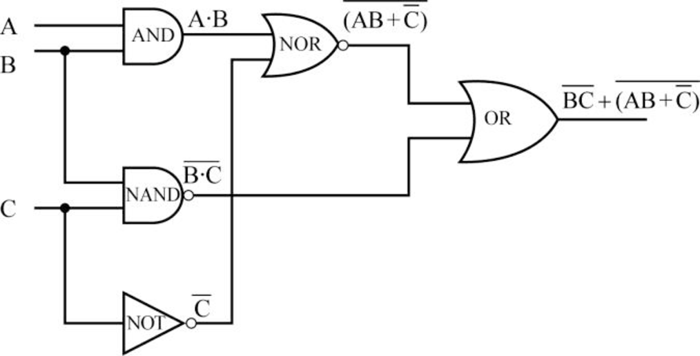
Behavior of the circuit:
- From the above circuit diagram,
- First, the inputs A and B are passed to AND gate to perform the product of A and B and produce the output as
- Next, pass the same input B from the AND gate, and input C is passed in the NAND gate to perform the inverse of product of B and C and produce the output as
- Next, pass the same input C from the NAND gate to NOT gate, to perform the inverse of C to produce the output as
- Next, pass the output of AND gate and output of NOT gate as the input to NOR gate to perform the inverse of sum of “
- Finally, the output of NOR gate and output of NAND gate is passed as the input of OR gate.
- Therefore, “
- Therefore, “
- First, the inputs A and B are passed to AND gate to perform the product of A and B and produce the output as
Truth table for the above circuit diagram:
Step 1:
- The inputs are A, B, and C for the circuit diagram:
| A | B | C | |||||
| 0 | 0 | 0 | |||||
| 0 | 0 | 1 | |||||
| 0 | 1 | 0 | |||||
| 0 | 1 | 1 | |||||
| 1 | 0 | 0 | |||||
| 1 | 0 | 1 | |||||
| 1 | 1 | 0 | |||||
| 1 | 1 | 1 |
Step 2:
- When the inputs are A as 0, B as 0, and C as 0:
| A | B | C | |||||
| 0 | 0 | 0 | 0 | 1 | 1 | 0 | 1 |
| 0 | 0 | 1 | |||||
| 0 | 1 | 0 | |||||
| 0 | 1 | 1 | |||||
| 1 | 0 | 0 | |||||
| 1 | 0 | 1 | |||||
| 1 | 1 | 0 | |||||
| 1 | 1 | 1 |
- First, the inputs A as 0 and B as 0 are passed to AND gate to perform the product of 0 and 0 and produce the output as
- Next, pass the same input B as 0 from the AND gate
- Next, pass the same input C as 0 from the NAND gate
- Next, pass the output of AND gate and output of NOT gate as the input for NOR gate to perform the inverse of sum of “0” and “1”, and produce the output as
- Finally, the output of NOR gate and output of NAND gate is passed as the input of OR gate.
- Therefore, “0” and “1” are passed as input to OR gate and produce the output as
- Therefore, “0” and “1” are passed as input to OR gate and produce the output as
Step 3:
- When the inputs are A as 0, B as 0, and C as 1:
| A | B | C | |||||
| 0 | 0 | 0 | 0 | 1 | 1 | 0 | 1 |
| 0 | 0 | 1 | 0 | 1 | 0 | 1 | 1 |
| 0 | 1 | 0 | |||||
| 0 | 1 | 1 | |||||
| 1 | 0 | 0 | |||||
| 1 | 0 | 1 | |||||
| 1 | 1 | 0 | |||||
| 1 | 1 | 1 |
- First, the inputs A as 0 and B as 0 are passed to AND gate to perform the product of 0 and 0 and produce the output as
- Next, pass the same input B as 0 from the AND gate
- Next, pass the same input C as 1 from the NAND gate
- Next, pass the output of AND gate and output of NOT gate as the input for NOR gate to perform the inverse of sum of “0” and “0” and produces the output as
- Finally, the output of NOR gate and output of NAND gate is passed as the input of OR gate.
- Therefore, “1” and “1” are passed as input to OR gate and produce the output as
- Therefore, “1” and “1” are passed as input to OR gate and produce the output as
Step 4:
- When the inputs are A as 0, B as 1, and C as 0:
| A | B | C | |||||
| 0 | 0 | 0 | 0 | 1 | 1 | 0 | 1 |
| 0 | 0 | 1 | 0 | 1 | 0 | 1 | 1 |
| 0 | 1 | 0 | 0 | 1 | 1 | 0 | 1 |
| 0 | 1 | 1 | |||||
| 1 | 0 | 0 | |||||
| 1 | 0 | 1 | |||||
| 1 | 1 | 0 | |||||
| 1 | 1 | 1 |
- First, the inputs A as 0 and B as 1 are passed to AND gate to perform the product of 0 and 1 and produce the output as
- Next, pass the same input B as 1 from the AND gate
- Next, pass the same input C as 0 from the NAND gate
- Next, pass the output of AND gate and output of NOT gate as the input for NOR gate to perform the inverse of sum of “0” and “1” and produces the output as
- Finally, the output of NOR gate and output of NAND gate are passed as the input of OR gate.
- Therefore, “0” and “1” are passed as input to OR gate and produce the output as
- Therefore, “0” and “1” are passed as input to OR gate and produce the output as
Step 5:
- When the inputs are A as 0, B as 1, and C as 1:
| A | B | C | |||||
| 0 | 0 | 0 | 0 | 1 | 1 | 0 | 1 |
| 0 | 0 | 1 | 0 | 1 | 0 | 1 | 1 |
| 0 | 1 | 0 | 0 | 1 | 1 | 0 | 1 |
| 0 | 1 | 1 | 0 | 0 | 0 | 1 | 1 |
| 1 | 0 | 0 | |||||
| 1 | 0 | 1 | |||||
| 1 | 1 | 0 | |||||
| 1 | 1 | 1 |
- First, the inputs A as 0 and B as 1 are passed to AND gate to perform the product of 0 and 1 and produce the output as
- Next, pass the same input B as 1 from the AND gate
- Next, pass the same input C as 1 from the NAND gate
- Next, pass the output of AND gate and output of NOT gate as the input for NOR gate to perform the inverse of sum of “0” and “0” and produces the output as
- Finally, the output of NOR gate and output of NAND gate are passed as the input of OR gate.
- Therefore, “1” and “0” are passed as input to OR gate and produce the output as
- Therefore, “1” and “0” are passed as input to OR gate and produce the output as
Step 6:
- When the inputs are A as 1, B as 0, and C as 0:
| A | B | C | |||||
| 0 | 0 | 0 | 0 | 1 | 1 | 0 | 1 |
| 0 | 0 | 1 | 0 | 1 | 0 | 1 | 1 |
| 0 | 1 | 0 | 0 | 1 | 1 | 0 | 1 |
| 0 | 1 | 1 | 0 | 0 | 0 | 1 | 1 |
| 1 | 0 | 0 | 0 | 1 | 1 | 0 | 1 |
| 1 | 0 | 1 | |||||
| 1 | 1 | 0 | |||||
| 1 | 1 | 1 |
- First, the inputs A as 1 and B as 0 are passed to AND gate to perform the product of 0 and 1 and produce the output as
- Next, pass the same input B as 0 from the AND gate
- Next, pass the same input C as 0 from the NAND gate
- Next, pass the output of AND gate and output of NOT gate as the input for NOR gate to perform the inverse of sum of “0” and “1” and produces the output as
- Finally, the output of NOR gate and output of NAND gate are passed as the input of OR gate.
- Therefore, “0” and “1” are passed as input to OR gate and produce the output as
- Therefore, “0” and “1” are passed as input to OR gate and produce the output as
Step 7:
- When the inputs are A as 1, B as 0, and C as 1:
| A | B | C | |||||
| 0 | 0 | 0 | 0 | 1 | 1 | 0 | 1 |
| 0 | 0 | 1 | 0 | 1 | 0 | 1 | 1 |
| 0 | 1 | 0 | 0 | 1 | 1 | 0 | 1 |
| 0 | 1 | 1 | 0 | 0 | 0 | 1 | 1 |
| 1 | 0 | 0 | 0 | 1 | 1 | 0 | 1 |
| 1 | 0 | 1 | 0 | 1 | 0 | 1 | 1 |
| 1 | 1 | 0 | |||||
| 1 | 1 | 1 |
- First, the inputs A as 1 and B as 0 are passed to AND gate to perform the product of 0 and 1 and produce the output as
- Next, pass the same input B as 0 from the AND gate
- Next, pass the same input C as 1 from the NAND gate
- Next, pass the output of AND gate and output of NOT gate as the input for NOR gate to perform the inverse of sum of “0” and “0” and produces the output as
- Finally, the output of NOR gate and output of NAND gate are passed as the input of OR gate.
- Therefore, “1” and “1” are passed as input to OR gate and produce the output as
- Therefore, “1” and “1” are passed as input to OR gate and produce the output as
Step 8:
- When the inputs are A as 1, B as 1, and C as 0:
| A | B | C | |||||
| 0 | 0 | 0 | 0 | 1 | 1 | 0 | 1 |
| 0 | 0 | 1 | 0 | 1 | 0 | 1 | 1 |
| 0 | 1 | 0 | 0 | 1 | 1 | 0 | 1 |
| 0 | 1 | 1 | 0 | 0 | 0 | 1 | 1 |
| 1 | 0 | 0 | 0 | 1 | 1 | 0 | 1 |
| 1 | 0 | 1 | 0 | 1 | 0 | 1 | 1 |
| 1 | 1 | 0 | 1 | 1 | 1 | 0 | 1 |
| 1 | 1 | 1 |
- First, the inputs A as 1 and B as 1 are passed to AND gate to perform the product of 1 and 1 and produce the output as
- Next, pass the same input B as 1 from the AND gate
- Next, pass the same input C as 0 from the NAND gate
- Next, pass the output of AND gate and output of NOT gate as the input for NOR gate to perform the inverse of sum of “1” and “1” and produces the output as
- Finally, the output of NOR gate and output of NAND gate are passed as the input of OR gate.
- That is, “0” and “1” are passed as input to OR gate and produce the output as
- That is, “0” and “1” are passed as input to OR gate and produce the output as
Step 9:
- When the inputs are A as 1, B as 1, and C as 1:
| A | B | C | |||||
| 0 | 0 | 0 | 0 | 1 | 1 | 0 | 1 |
| 0 | 0 | 1 | 0 | 1 | 0 | 1 | 1 |
| 0 | 1 | 0 | 0 | 1 | 1 | 0 | 1 |
| 0 | 1 | 1 | 0 | 0 | 0 | 1 | 1 |
| 1 | 0 | 0 | 0 | 1 | 1 | 0 | 1 |
| 1 | 0 | 1 | 0 | 1 | 0 | 1 | 1 |
| 1 | 1 | 0 | 1 | 1 | 1 | 0 | 1 |
| 1 | 1 | 1 | 1 | 0 | 0 | 0 | 0 |
- First, the inputs A as 1 and B as 1 are passed to AND gate to perform the product of 1 and 1 and produce the output as
- Next, pass the same input B as 1 from the AND gate
- Next, pass the same input C as 1 from the NAND gate
- Next, pass the output of AND gate and output of NOT gate as the input for NOR gate to perform the inverse of sum of “1” and “0” and produces the output as
- Finally, the output of NOR gate and output of NAND gate are passed as the input of OR gate.
- Thus, “0” and “0” are passed as input to OR gate and produce the output as
- Thus, “0” and “0” are passed as input to OR gate and produce the output as
Therefore, the truth table for the given circuit is:
| A | B | C | |||||
| 0 | 0 | 0 | 0 | 1 | 1 | 0 | 1 |
| 0 | 0 | 1 | 0 | 1 | 0 | 1 | 1 |
| 0 | 1 | 0 | 0 | 1 | 1 | 0 | 1 |
| 0 | 1 | 1 | 0 | 0 | 0 | 1 | 1 |
| 1 | 0 | 0 | 0 | 1 | 1 | 0 | 1 |
| 1 | 0 | 1 | 0 | 1 | 0 | 1 | 1 |
| 1 | 1 | 0 | 1 | 1 | 1 | 0 | 1 |
| 1 | 1 | 1 | 1 | 0 | 0 | 0 | 0 |
Want to see more full solutions like this?
Subscribe now to access step-by-step solutions to millions of textbook problems written by subject matter experts!
Students have asked these similar questions
CPS 2231 - Computer Programming – Spring 2025
City Report Application
-
Due Date:
Concepts: Classes and Objects, Reading from a file and generating report
Point value: 40 points.
The purpose of this project is to give students exposure to object-oriented design and programming
using classes in a realistic application that involves arrays of objects and generating reports.
Assignment Instructions:
You are tasked with developing a program to use city data from an online database and generate a
city details report.
1) Create a new Project in Eclipse called "HW7”.
2) Create a class "City.java" in the project and implement the UML diagram shown below and add
comments to your program.
3) The logic for the method "getCityCategory" of City Class is below:
a. If the population of a city is greater than 10000000, then the method returns "MEGA"
b. If the population of a city is greater than 1000000 and less than 10000000, then the
method returns "LARGE"
c. If the population of a city is greater…
Please calculate the average best-case IPC attainable on this code with a 2-wide, in-order, superscalar machine:
ADD X1, X2, X3
SUB X3, X1, 0x100
ORR X9, X10, X11
ADD X11, X3, X2
SUB X9, X1, X3
ADD X1, X2, X3
AND X3, X1, X9
ORR X1, X11, X9
SUB X13, X14, X15
ADD X16, X13, X14
Outline the overall steps for configuring and securing Linux servers
Consider and describe how a mixed Operating System environment will affect what you have to do to protect the company assets
Describe at least three technologies that will help to protect CIA of data on Linux systems
Chapter 4 Solutions
Computer Science Illuminated
Ch. 4 - Prob. 1ECh. 4 - Prob. 2ECh. 4 - Prob. 3ECh. 4 - Prob. 4ECh. 4 - Prob. 5ECh. 4 - Prob. 6ECh. 4 - Prob. 7ECh. 4 - Prob. 8ECh. 4 - Prob. 9ECh. 4 - Prob. 10E
Ch. 4 - Prob. 11ECh. 4 - Prob. 12ECh. 4 - Prob. 13ECh. 4 - Prob. 14ECh. 4 - Prob. 15ECh. 4 - Prob. 16ECh. 4 - Prob. 17ECh. 4 - Prob. 18ECh. 4 - Prob. 19ECh. 4 - Prob. 20ECh. 4 - Prob. 21ECh. 4 - Prob. 22ECh. 4 - Prob. 23ECh. 4 - Prob. 24ECh. 4 - Prob. 25ECh. 4 - Prob. 26ECh. 4 - Prob. 27ECh. 4 - Prob. 28ECh. 4 - Prob. 29ECh. 4 - Prob. 30ECh. 4 - Prob. 31ECh. 4 - Prob. 32ECh. 4 - Prob. 33ECh. 4 - Prob. 34ECh. 4 - Prob. 35ECh. 4 - Prob. 36ECh. 4 - Prob. 37ECh. 4 - Prob. 38ECh. 4 - Prob. 39ECh. 4 - Prob. 40ECh. 4 - Prob. 41ECh. 4 - Prob. 42ECh. 4 - Prob. 43ECh. 4 - Prob. 44ECh. 4 - Prob. 45ECh. 4 - Prob. 46ECh. 4 - Prob. 47ECh. 4 - Prob. 48ECh. 4 - Prob. 49ECh. 4 - Prob. 50ECh. 4 - Prob. 51ECh. 4 - Prob. 52ECh. 4 - Prob. 53ECh. 4 - Prob. 54ECh. 4 - Prob. 55ECh. 4 - Prob. 56ECh. 4 - Prob. 57ECh. 4 - Prob. 58ECh. 4 - Prob. 59ECh. 4 - Prob. 60ECh. 4 - Prob. 61ECh. 4 - Prob. 62ECh. 4 - Prob. 63ECh. 4 - Prob. 64ECh. 4 - Prob. 65ECh. 4 - Prob. 66ECh. 4 - Prob. 67ECh. 4 - Prob. 68ECh. 4 - Prob. 69ECh. 4 - Prob. 70ECh. 4 - Prob. 71ECh. 4 - Prob. 72ECh. 4 - Prob. 73ECh. 4 - Prob. 1TQCh. 4 - Prob. 2TQCh. 4 - Prob. 3TQCh. 4 - Prob. 4TQ
Knowledge Booster


Learn more about
Need a deep-dive on the concept behind this application? Look no further. Learn more about this topic, computer-science and related others by exploring similar questions and additional content below.Similar questions
- Node.js, Express, Nunjucks, MongoDB, and Mongoose There are a couple of programs similar to this assignment given in the lecture notes for the week that discusses CRUD operations. Specifically, the Admin example and the CIT301 example both have index.js code and nunjucks code similar to this assignment. You may find some of the other example programs useful as well. It would ultimately save you time if you have already studied these programs before giving this assignment a shot. Either way, hopefully you'll start early and you've kept to the schedule in terms of reading the lecture notes. You will need to create a database named travel using compass, then create a collection named trips. Use these names; your code must work with my database. The trips documents should then be imported unto the trips collection by importing the JSON file containing all the data as linked below. The file itself is named trips.json, and is available on the course website in the same folder as this…arrow_forwardusing r languagearrow_forwardusing r languagearrow_forward
- using r languagearrow_forwardWrite a short paper (1 page/about 500 words) summarizing what we as System Admins can do to protect the CIA of our servers. Outline the overall steps for configuring and securing Linux servers Consider and describe how a mixed Operating System environment will affect what you have to do to protect the company assets Describe at least three technologies that will help to protect CIA of data on Linux systems Required Resourcesarrow_forwardusing r language Estimate the MSE of the level k trimmed means for random samples of size 20 generated from a standard Cauchy distribution. (The target parameter θis the center or median; the expected value does not exist.) Summarize the estimates of MSE in a table for k= 1,2,...,9arrow_forward
- using r language Estimate the MSE of the level k trimmed means for random samples of size 20 generated from a standard Cauchy distribution. (The target parameter θis the center or median; the expected value does not exist.) Summarize the estimates of MSE in a table for k= 1,2,...,9arrow_forwardusing r language The data law82 in bootstrap library contains LSAT and GPA for 82 law schools. Compute a 95% bootstrap t confidence interval estimates for the correlation statisticsarrow_forwardusing r language The data law82 in bootstrap library contains LSAT and GPA for 82 law schools. Compute a 95% bootstrap t confidence interval estimates for the correlation statisticsarrow_forward
- using r langauge The data law82 in bootstrap library contains LSAT and GPA for 82 law schools. Compute and compare the three 95% bootstrap confidence interval estimates for the correlation statistics.arrow_forwardWhat is the number of derangements of size k from the set {1,2,...n} to the set {1,2,...n} so that f(x) != x exactly k times with 1 <= k <= narrow_forwardTrace a State Space Tree introduced in the Chapter 5.1 using algorithms depth_first_search (page 205), checknode (page 207), and expand (page 210). Assume that State Space Tree is a two-level full binary tree (root is level 0). Node #2 (according to notation used in the Figure 5.1, page 204) is non-promising. Count the number of steps performed by each of those three algorithms. Consider execution of instructions like "visit node" or execution of "promising function" as one step, "write a solution" as an exit call. Note: no need to print or a draw a whole tree. Just provide three numbers as an answerarrow_forward
arrow_back_ios
SEE MORE QUESTIONS
arrow_forward_ios
Recommended textbooks for you
 Database System ConceptsComputer ScienceISBN:9780078022159Author:Abraham Silberschatz Professor, Henry F. Korth, S. SudarshanPublisher:McGraw-Hill Education
 Starting Out with Python (4th Edition)Computer ScienceISBN:9780134444321Author:Tony GaddisPublisher:PEARSON
 Digital Fundamentals (11th Edition)Computer ScienceISBN:9780132737968Author:Thomas L. FloydPublisher:PEARSON
 C How to Program (8th Edition)Computer ScienceISBN:9780133976892Author:Paul J. Deitel, Harvey DeitelPublisher:PEARSON
 Database Systems: Design, Implementation, & Manag...Computer ScienceISBN:9781337627900Author:Carlos Coronel, Steven MorrisPublisher:Cengage Learning
 Programmable Logic ControllersComputer ScienceISBN:9780073373843Author:Frank D. PetruzellaPublisher:McGraw-Hill Education
Database System Concepts
Computer Science
ISBN:9780078022159
Author:Abraham Silberschatz Professor, Henry F. Korth, S. Sudarshan
Publisher:McGraw-Hill Education
Starting Out with Python (4th Edition)
Computer Science
ISBN:9780134444321
Author:Tony Gaddis
Publisher:PEARSON
Digital Fundamentals (11th Edition)
Computer Science
ISBN:9780132737968
Author:Thomas L. Floyd
Publisher:PEARSON
C How to Program (8th Edition)
Computer Science
ISBN:9780133976892
Author:Paul J. Deitel, Harvey Deitel
Publisher:PEARSON
Database Systems: Design, Implementation, & Manag...
Computer Science
ISBN:9781337627900
Author:Carlos Coronel, Steven Morris
Publisher:Cengage Learning
Programmable Logic Controllers
Computer Science
ISBN:9780073373843
Author:Frank D. Petruzella
Publisher:McGraw-Hill Education
Boolean Algebra - Digital Logic and Logic Families - Industrial Electronics; Author: Ekeeda;https://www.youtube.com/watch?v=u7XnJos-_Hs;License: Standard YouTube License, CC-BY
Boolean Algebra 1 – The Laws of Boolean Algebra; Author: Computer Science;https://www.youtube.com/watch?v=EPJf4owqwdA;License: Standard Youtube License