ANALYSIS+DESIGN OF LINEAR CIRCUITS(LL)
8th Edition
ISBN: 9781119235385
Author: Thomas
Publisher: WILEY
expand_more
expand_more
format_list_bulleted
Videos
Textbook Question
Chapter 4, Problem 4.37P
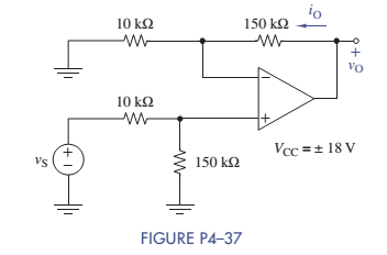
For the circuit in Figure P4-37:
(a) Find
(b) Find
Expert Solution & Answer
Want to see the full answer?
Check out a sample textbook solution
Students have asked these similar questions
the first part is
the second part
write your answer such as: (AND, OR, INVERTER, NAND, NOR)
D₁
AK
D,
R₁
B
K
First Part?
the third part is
, and the total are
R4
R7
Output
R5
R₁
T
R6
R3
-UBB
Second Part?
Third Part?
Total?
A multistage amplifier has six stages each of which has a power gain of 40. what is the
- Total gain of the amplifier in db
?
ii- If the negative feedback of 15db is employed, find the resultant gain
9.36 Consider the finite-state machine logic implementation in Figure P9.36.
(a) Determine the next-state and output logic expressions.
(b) Determine the number of possible states.
J1
Clk
K₁
101
Ут
J2
Clk
K₂
Clk
Figure P9.36
0
y2
10
Chapter 4 Solutions
ANALYSIS+DESIGN OF LINEAR CIRCUITS(LL)
Ch. 4 - Find the voltage gain vO/vS and current gain iO/ix...Ch. 4 - Prob. 4.2PCh. 4 - Prob. 4.3PCh. 4 - Prob. 4.4PCh. 4 - Find the voltage gain vO/vS in Figure P4-5.Ch. 4 - Find the voltage gain vO/vS in Figure P4-6.Ch. 4 - Find an expression for the current gain iO/iS in...Ch. 4 - Prob. 4.8PCh. 4 - Prob. 4.9PCh. 4 - Find an expression for the voltage gain vO/vs in...
Ch. 4 - Prob. 4.12PCh. 4 - In the circuit of Figure P4-13, the VCVS has of...Ch. 4 - Prob. 4.14PCh. 4 - (a) Find the Thévenin equivalent circuit that the...Ch. 4 - Prob. 4.16PCh. 4 - Prob. 4.18PCh. 4 - Prob. 4.19PCh. 4 - The circuit parameters in figure P4-21 are...Ch. 4 - The circuit parameters in Figure P4-21 are...Ch. 4 - The parameters of the transistor in Figure P4-23...Ch. 4 - Prob. 4.25PCh. 4 - Find the voltage gain of each OP AMP circuit shown...Ch. 4 - Considering simplicity and standard 10 tolerance...Ch. 4 - Two OP AMP circuits are shown in Figure P4-28....Ch. 4 - Prob. 4.29PCh. 4 - What is the range of the gain vO/vS in Figure...Ch. 4 - Using only one OP AMP, design a circuit that...Ch. 4 - Design a circuit using only one OP AMP that...Ch. 4 - Prob. 4.36PCh. 4 - For the circuit in Figure P4-37: (a) Find vO in...Ch. 4 - A young designer needed to amplify a 2-V signal by...Ch. 4 - Design two circuits to produce the following...Ch. 4 - Design a noninverting summer for five inputs with...Ch. 4 - For the circuit in Figure P4-41: Find vO in terms...Ch. 4 - The input-output relationship for a three-input...Ch. 4 - Find vo in terms of the inputs v1,v2, and v3 in...Ch. 4 - Prob. 4.44PCh. 4 - Prob. 4.45PCh. 4 - Prob. 4.46PCh. 4 - Prob. 4.47PCh. 4 - It is claimed that vO=vS when the switch is closed...Ch. 4 - Prob. 4.49PCh. 4 - Prob. 4.50PCh. 4 - Use node-voltage analysis in Figure P4-51 to show...Ch. 4 - Prob. 4.52PCh. 4 - Prob. 4.53PCh. 4 - For the block diagram of Figure P4-54: Find an...Ch. 4 - For the block diagram of Figure P4-55: Find an...Ch. 4 - For the circuit in Figure P4-56: Find vO in terms...Ch. 4 - Prob. 4.57PCh. 4 - Onan exam, students were asked to design an...Ch. 4 - Prob. 4.59PCh. 4 - For the circuit of Figure P4-60: Use node-voltage...Ch. 4 - Prob. 4.61PCh. 4 - Design a single OP AMP amplifier with a voltage...Ch. 4 - Design an OP AMP amplifier with a voltage gain of...Ch. 4 - Using a single OP AMP, design a circuit with...Ch. 4 - Design a differential amplifier with inputs v1 and...Ch. 4 - Using no more than two OP AMPs, design an OP AMP...Ch. 4 - Design a two-input noninverting summer that will...Ch. 4 - Design a three-input noninverting summer that will...Ch. 4 - Design a cascaded OP AMP circuit that will produce...Ch. 4 - Design a cascaded OP AMP circuit that will produce...Ch. 4 - Using the instrumentation amplifier shown in...Ch. 4 - Prob. 4.73PCh. 4 - Design a circuit that can produce vO=2000vTR2.6V...Ch. 4 - A requirement exists for an OP AMP circuit with...Ch. 4 - A requirement exists for an OP AMP circuit to...Ch. 4 - A particular application requires that an...Ch. 4 - Prob. 4.78PCh. 4 - The full-scale output of a six-bit DAC is 10.0 V....Ch. 4 - An R2R DAC is shown in Figure P4-80. The digital...Ch. 4 - A fifth bit is added to the R-2R DAC shown in...Ch. 4 - Prob. 4.82PCh. 4 - Prob. 4.83PCh. 4 - A small pressure transducer has the...Ch. 4 - A medical grade pressure transducer has been...Ch. 4 - The acid/alkaline balance of a fluid is measured...Ch. 4 - A photoresistor varies from 10 in bright sunlight...Ch. 4 - Your engineering firm needs an instrumentation...Ch. 4 - Prob. 4.90PCh. 4 - Prob. 4.92PCh. 4 - Prob. 4.93PCh. 4 - A five-bit flash ADC in Figure P4-94 uses a...Ch. 4 - Bipolar Power Supply Voltages The circuit in...Ch. 4 - Thermometer Design Problem There is a need to...Ch. 4 - High Bias Design Problem A particular pressure...Ch. 4 - Prob. 4.99IPCh. 4 - OP AMP Circuit Analysis and Design Find the...Ch. 4 - Instrumentation Amplifier with Alarm Strain gauges...
Knowledge Booster


Learn more about
Need a deep-dive on the concept behind this application? Look no further. Learn more about this topic, electrical-engineering and related others by exploring similar questions and additional content below.Similar questions
- 9.34 Consider the finite-state machine logic implementation in Figure P9.34. (a) Determine the next-state and output logic expressions. (b) Determine the number of possible states. (c) Construct a state assigned table. (d) Construct a state table. (e) Construct a state diagram. (f) Determine the function of the finite-state machine. T₁ x Clk Figure P9.34 Q Clk Q الا T₂ Q 32 Clk Q T3 Q Clk Q Узarrow_forward9.35 Consider the finite-state machine logic implementation in Figure P9.35. (a) Determine the next-state and output logic expressions. (b) Determine the number of possible states. (c) Construct a state assigned table. (d) Construct a state table. (e) Construct a state diagram. (f) Determine the function of the finite-state machine. Clk J Clk K₁ 10 Ут J2 Clk K₂ 10 32 Figure P9.35arrow_forward9.56 Using JK flip-flops, design a synchronous counter that counts in the sequence 1, 3, 0, 2, 1, ... The counter counts only when its enable input x is equal to 1; otherwise, the counter is idle.arrow_forward
- 9.65 Using T flip-flops, design a synchronous counter that counts in the sequence 0, 2, 4, 6, 0, ... The counter counts only when its enable input x is equal to 1; otherwise, the counter is idle.arrow_forward2 Using D flip-flops, design a synchronous counter that counts in the sequence 1, 4, 7, 1, The counter counts only when its enable input x is equal to 1; otherwise, the counter is idle.arrow_forwardQ1: Write a VHDL code to implement the finite state machine described in the state diagram shown below. Clk D 0 CIK Q D 0 Cik Q =arrow_forward
- Q1: Consider the finite state machine logic implementation in Fig. shown below: Construct the state diagram. Repeat the circuit design using j-k flip flop. r" Clk Y D' Y, Clk Q D Clk 10 0 22 3'2arrow_forwardQ: Write a VHDL code to implement the finite state machine described in the state diagram shown below. T 2 Clk Q Clk T₂ 0 la Clk T3 Q Cik 0arrow_forwardDo you happen to know what is the complete circuit?arrow_forward
- b) Draw the magnitude and phase bode plot c) Given Cdb=0.02pF, how will the frequency response change, draw the resulting magnitude and phase bode plotplz help me to solve part b and c.arrow_forwardMedium 1 is a lossless dielectric (ε₁, μ₁ = μo, σ₁ = 0) Medium 2 is a perfect electric conductor (PEC) ( 2 = 0, μ2 = μo, σ₂ = ∞) [ Moσ = 0] [ε0 μ₁ σ₂ = ∞ ] (J=σE is finite, E = 0) E(z) Exe² +Пe₁²] 1. For the case εr] = λι = = E2(z)-0 - 1 (vacuum), E₁x 1 V/m and a frequency f = 500 MHz determine: n₁ = 12= 2. Determine: r = T= 3. Using this I show that the total electric field E₁0(z) in region 1 can be written as: E(z) = -2jE, sin(2лz/λ)✰ 4. The magnitude E10(z) will show an interference pattern. The SWR (standing wave ratio) is the Emax/Emin ratio of the magnitude of the total electric field in region 1. What is the SWR? E (z) = 2|E|sin(2лz/2₁)| E" (z) SWR A Imax E(z) Imin 1+r 1-|| tot 5. Roughly SKETCH the magnitude of E10(z) and E20(z) on the graph below. E₁tot(z) tot E20(z) -0.40 -0.30 -0.ło z=0 +0.1b +0.20arrow_forwardwould anyone be able to tell me the amount of wire needed for this electrical plan in this house? and if possible would anyone be able to tell me the amount of any other materials needed (wire sizes, box sizes/styles)arrow_forward
arrow_back_ios
SEE MORE QUESTIONS
arrow_forward_ios
Recommended textbooks for you
 Introductory Circuit Analysis (13th Edition)Electrical EngineeringISBN:9780133923605Author:Robert L. BoylestadPublisher:PEARSON
 Delmar's Standard Textbook Of ElectricityElectrical EngineeringISBN:9781337900348Author:Stephen L. HermanPublisher:Cengage Learning
 Programmable Logic ControllersElectrical EngineeringISBN:9780073373843Author:Frank D. PetruzellaPublisher:McGraw-Hill Education
 Fundamentals of Electric CircuitsElectrical EngineeringISBN:9780078028229Author:Charles K Alexander, Matthew SadikuPublisher:McGraw-Hill Education
 Electric Circuits. (11th Edition)Electrical EngineeringISBN:9780134746968Author:James W. Nilsson, Susan RiedelPublisher:PEARSON
 Engineering ElectromagneticsElectrical EngineeringISBN:9780078028151Author:Hayt, William H. (william Hart), Jr, BUCK, John A.Publisher:Mcgraw-hill Education,
Introductory Circuit Analysis (13th Edition)
Electrical Engineering
ISBN:9780133923605
Author:Robert L. Boylestad
Publisher:PEARSON
Delmar's Standard Textbook Of Electricity
Electrical Engineering
ISBN:9781337900348
Author:Stephen L. Herman
Publisher:Cengage Learning
Programmable Logic Controllers
Electrical Engineering
ISBN:9780073373843
Author:Frank D. Petruzella
Publisher:McGraw-Hill Education
Fundamentals of Electric Circuits
Electrical Engineering
ISBN:9780078028229
Author:Charles K Alexander, Matthew Sadiku
Publisher:McGraw-Hill Education
Electric Circuits. (11th Edition)
Electrical Engineering
ISBN:9780134746968
Author:James W. Nilsson, Susan Riedel
Publisher:PEARSON
Engineering Electromagnetics
Electrical Engineering
ISBN:9780078028151
Author:Hayt, William H. (william Hart), Jr, BUCK, John A.
Publisher:Mcgraw-hill Education,
Lead and lag compensation using Bode diagrams; Author: John Rossiter;https://www.youtube.com/watch?v=UBE-Tp173vk;License: Standard Youtube License