ANALYSIS+DESIGN OF LINEAR CIRCUITS(LL)
8th Edition
ISBN: 9781119235385
Author: Thomas
Publisher: WILEY
expand_more
expand_more
format_list_bulleted
Concept explainers
Videos
Textbook Question
Chapter 4, Problem 4.51P
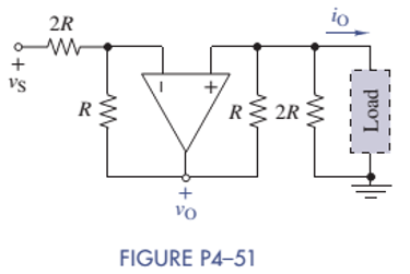
Use node-voltage analysis in Figure P4-51 to show that
Expert Solution & Answer
Want to see the full answer?
Check out a sample textbook solution
Students have asked these similar questions
Design a counter to count-up from 2 to 7 using three of
D Flip Flops
(3) 3-Bit Count up (3 to 5) Using D Flip-Flop:
The State Equation of D Flip-Flop:
Q(t+1)=D(t) => Dn=Qn
Present State
D Flip-Flop
Next State
n
Q2p Q1p Q0p
3
0 1
1
1
Q2n Q1n Q0n D2 D1 D0
0 0 1 0 0
4
1
0
0
1
0
1
1 0
1
5
1 0
1
0
1
1
01
1
D2-Sum(3,4) and don't care X-Sum(0,1,2,6,7)
D1=Sum(5) and don't care X=Sum(0,1,2,6,7)
D0=Sum(4,5) and don't care X=Sum(0,1,2,6,7)
Using K-map to simplify the functions:
D2=Q1+Q0'
D1=Q1'QO
DO=Q1'
XOX
XOX
Q2 10
Q2 01
Q2 1xx
Q0
QO
Qo
D2 Q2
>CK
Q2
D1 Q1
BCD
CK
Q1
DO QF
►CK
Q0
☐ Present State Next State D Flip-Flop
n Q2p Q1p Q0p Q2n Q1n Q0n D2 D1 D0
2 0 1
0
0 1 1 0 1 1
3 0
1
1
1
0
0 1 00
4
1
0
0
1
0
1
1
0
1
5
1
0
1
1
1
0
1 1
0
6
1
1
0
0
1
0
0
1
0
D2
D2=Sum(3,4,5), X=Sum(0,1,7)
D1
Q2
1
Q1
1
0
☑
0
Qo
D2=Q0+Q1'
✗
0
Q1
Consider the following 4×1 multiplexer with inputs:
w0=2, w1=1, w2=x2' and w3=0
And with switches:
S1 x1 and S0=x0
What is the multiplexer output f as a function of x2, x1
and x0?
I need help adding a capacitor and a Zener diode to my circuit. I’m looking for a simple sketch or diagram showing how to connect them. i want diagram with final circuit after adding the zener diad and capacitor. don't do calclution or anything. thanks
Chapter 4 Solutions
ANALYSIS+DESIGN OF LINEAR CIRCUITS(LL)
Ch. 4 - Find the voltage gain vO/vS and current gain iO/ix...Ch. 4 - Prob. 4.2PCh. 4 - Prob. 4.3PCh. 4 - Prob. 4.4PCh. 4 - Find the voltage gain vO/vS in Figure P4-5.Ch. 4 - Find the voltage gain vO/vS in Figure P4-6.Ch. 4 - Find an expression for the current gain iO/iS in...Ch. 4 - Prob. 4.8PCh. 4 - Prob. 4.9PCh. 4 - Find an expression for the voltage gain vO/vs in...
Ch. 4 - Prob. 4.12PCh. 4 - In the circuit of Figure P4-13, the VCVS has of...Ch. 4 - Prob. 4.14PCh. 4 - (a) Find the Thévenin equivalent circuit that the...Ch. 4 - Prob. 4.16PCh. 4 - Prob. 4.18PCh. 4 - Prob. 4.19PCh. 4 - The circuit parameters in figure P4-21 are...Ch. 4 - The circuit parameters in Figure P4-21 are...Ch. 4 - The parameters of the transistor in Figure P4-23...Ch. 4 - Prob. 4.25PCh. 4 - Find the voltage gain of each OP AMP circuit shown...Ch. 4 - Considering simplicity and standard 10 tolerance...Ch. 4 - Two OP AMP circuits are shown in Figure P4-28....Ch. 4 - Prob. 4.29PCh. 4 - What is the range of the gain vO/vS in Figure...Ch. 4 - Using only one OP AMP, design a circuit that...Ch. 4 - Design a circuit using only one OP AMP that...Ch. 4 - Prob. 4.36PCh. 4 - For the circuit in Figure P4-37: (a) Find vO in...Ch. 4 - A young designer needed to amplify a 2-V signal by...Ch. 4 - Design two circuits to produce the following...Ch. 4 - Design a noninverting summer for five inputs with...Ch. 4 - For the circuit in Figure P4-41: Find vO in terms...Ch. 4 - The input-output relationship for a three-input...Ch. 4 - Find vo in terms of the inputs v1,v2, and v3 in...Ch. 4 - Prob. 4.44PCh. 4 - Prob. 4.45PCh. 4 - Prob. 4.46PCh. 4 - Prob. 4.47PCh. 4 - It is claimed that vO=vS when the switch is closed...Ch. 4 - Prob. 4.49PCh. 4 - Prob. 4.50PCh. 4 - Use node-voltage analysis in Figure P4-51 to show...Ch. 4 - Prob. 4.52PCh. 4 - Prob. 4.53PCh. 4 - For the block diagram of Figure P4-54: Find an...Ch. 4 - For the block diagram of Figure P4-55: Find an...Ch. 4 - For the circuit in Figure P4-56: Find vO in terms...Ch. 4 - Prob. 4.57PCh. 4 - Onan exam, students were asked to design an...Ch. 4 - Prob. 4.59PCh. 4 - For the circuit of Figure P4-60: Use node-voltage...Ch. 4 - Prob. 4.61PCh. 4 - Design a single OP AMP amplifier with a voltage...Ch. 4 - Design an OP AMP amplifier with a voltage gain of...Ch. 4 - Using a single OP AMP, design a circuit with...Ch. 4 - Design a differential amplifier with inputs v1 and...Ch. 4 - Using no more than two OP AMPs, design an OP AMP...Ch. 4 - Design a two-input noninverting summer that will...Ch. 4 - Design a three-input noninverting summer that will...Ch. 4 - Design a cascaded OP AMP circuit that will produce...Ch. 4 - Design a cascaded OP AMP circuit that will produce...Ch. 4 - Using the instrumentation amplifier shown in...Ch. 4 - Prob. 4.73PCh. 4 - Design a circuit that can produce vO=2000vTR2.6V...Ch. 4 - A requirement exists for an OP AMP circuit with...Ch. 4 - A requirement exists for an OP AMP circuit to...Ch. 4 - A particular application requires that an...Ch. 4 - Prob. 4.78PCh. 4 - The full-scale output of a six-bit DAC is 10.0 V....Ch. 4 - An R2R DAC is shown in Figure P4-80. The digital...Ch. 4 - A fifth bit is added to the R-2R DAC shown in...Ch. 4 - Prob. 4.82PCh. 4 - Prob. 4.83PCh. 4 - A small pressure transducer has the...Ch. 4 - A medical grade pressure transducer has been...Ch. 4 - The acid/alkaline balance of a fluid is measured...Ch. 4 - A photoresistor varies from 10 in bright sunlight...Ch. 4 - Your engineering firm needs an instrumentation...Ch. 4 - Prob. 4.90PCh. 4 - Prob. 4.92PCh. 4 - Prob. 4.93PCh. 4 - A five-bit flash ADC in Figure P4-94 uses a...Ch. 4 - Bipolar Power Supply Voltages The circuit in...Ch. 4 - Thermometer Design Problem There is a need to...Ch. 4 - High Bias Design Problem A particular pressure...Ch. 4 - Prob. 4.99IPCh. 4 - OP AMP Circuit Analysis and Design Find the...Ch. 4 - Instrumentation Amplifier with Alarm Strain gauges...
Knowledge Booster


Learn more about
Need a deep-dive on the concept behind this application? Look no further. Learn more about this topic, electrical-engineering and related others by exploring similar questions and additional content below.Similar questions
- Question 3 AC Motor Drives [15]Calculate the instantaneous currents delivered by the inverter if the direct axiscurrent required at a particular instant is 8.66A and the quadrature current is5A. Derive all equations for the three currents.arrow_forwardA certain signal f(t) has the following PSD (assume 12 load): Sp (w) = new + 8(w) - 1.5) + (w + 1.5)] (a) What is the mean power in the bandwidth w≤2 rad/see? (b) What is the mean power in the bandwidth -1.9 to 0.99 rad/sec? Paress(w) dw 2ㅈ -arrow_forward(75 Marks) JA signal (t) is bond 7)(t)(t) and f(t), are band-limited to 1.2 kHz each. These signals are to be limited to 9.6 kHz, and three other signals transmitted by means of time-division multiplexing. Set up scheme for accomplishing this multiplexing requirement, with each signal sampled at its Nyquist rate. What must be the speed of the commutator (the output but ram-k bit/sec)? the minimum band width? (25 Marks)arrow_forward
- Draw the digital modulation outputs, ASK Amplitude Shift Keying) FSK (Frequency Shift Keying) and PSK (Phase Shift Keying). For baseband and carriet frequency as shown 101 wwwwwwwwwwww 010 BASESAND basband CARRIER Carralarrow_forwardplease show full working. I've included the solutionarrow_forwardcan you please show working and steps. The answer is 8kohms.arrow_forward
- PSD A certain signal f(t) has the following PSD (assume 12 load): | Sƒ(w) = π[e¯\w\ + 8(w − 2) + +8(w + 2)] (a) What is the mean power in the bandwidth w≤ 1 rad/sec? (b) What is the mean power in the bandwidth 0.99 to 1.01 rad/sec? (c) What is the mean power in the bandwidth 1.99 to 2.01 rad/sec? (d) What is the total mean power in (t)? Pav= + 2T SfLw) dw - SALW)arrow_forwardAn AM modulation waveform signal:- p(t)=(8+4 cos 1000πt + 4 cos 2000πt) cos 10000nt (a) Sketch the amplitude spectrum of p(t). (b) Find total power, sideband power and power efficiency. (c) Find the average power containing of each sideband.arrow_forwardCan you rewrite the solution because it is unclear? AM (+) = 8(1+ 0.5 cos 1000kt +0.5 ros 2000ks) = cos 10000 πt. 8 cos wat + 4 cos wit + 4 cos Wat coswet. -Jet jooort J11000 t = 4 e jqooort jgoort +4e + e +e j 12000rt. 12000 kt + e +e jooxt igoo t te (w) = 8ES(W- 100007) + 8IS (W-10000) USBarrow_forward
- Can you rewrite the solution because it is unclear? AM (+) = 8(1+0.5 cos 1000kt +0.5 ros 2000 thts) = cos 10000 πt. 8 cos wat + 4 cos wit + 4 cos Wat coswet. J4000 t j11000rt $14+) = 45 jqooort +4e + e + e j 12000rt. 12000 kt + e +e +e Le jsoort -; goon t te +e Dcw> = 885(W- 100007) + 8 IS (W-10000) - USBarrow_forwardCan you rewrite the solution because it is unclear? Q2 AM ①(+) = 8 (1+0.5 cos 1000πt +0.5 ros 2000kt) $4+) = 45 = *cos 10000 πt. 8 cos wat + 4 cosat + 4 cos Wat coswet. j1000016 +4e -j10000πt j11000Rt j gooort -j 9000 πt + e +e j sooort te +e J11000 t + e te j 12000rt. -J12000 kt + с = 8th S(W- 100007) + 8 IS (W-10000) <&(w) = USB -5-5 -4-5-4 b) Pc 2² = 64 PSB = 42 + 4 2 Pt Pc+ PSB = y = Pe c) Puss = PLSB = = 32 4² = 8 w 32+ 8 = × 100% = 140 (1)³×2×2 31 = 20% x 2 = 3w 302 USB 4.5 5 5.6 6 ms Ac = 4 mi = 0.5 mz Ac = 4 ५ M2 = =0.5arrow_forwardA. Draw the waveform for the following binary sequence using Bipolar RZ, Bipolar NRZ, and Manchester code. Data sequence= (00110100) B. In a binary PCM system, the output signal-to-quantization ratio is to be hold to a minimum of 50 dB. If the message is a single tone with fm-5 kHz. Determine: 1) The number of required levels, and the corresponding output signal-to-quantizing noise ratio. 2) Minimum required system bandwidth.arrow_forward
arrow_back_ios
SEE MORE QUESTIONS
arrow_forward_ios
Recommended textbooks for you
 Delmar's Standard Textbook Of ElectricityElectrical EngineeringISBN:9781337900348Author:Stephen L. HermanPublisher:Cengage Learning
Delmar's Standard Textbook Of Electricity
Electrical Engineering
ISBN:9781337900348
Author:Stephen L. Herman
Publisher:Cengage Learning
Superposition Theorem; Author: The Organic Chemistry Tutor;https://www.youtube.com/watch?v=EX52BuZxpQM;License: Standard Youtube License