Concept explainers
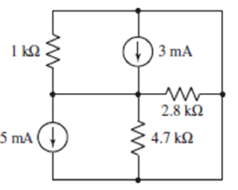
Although drawn so that it may not appear obvious at first glance, the circuit of Fig. 3.74 is in fact a single-node-pair circuit, (a) Determine the power absorbed by each resistor, (b) Determine the power supplied by each current source, (c) Show that the sum of the absorbed power calculated in (a) is equal to the sum of the supplied power calculated in (b).

FIGURE 3.74
(a)
Find power absorbed by each resistor.
Answer to Problem 34E
Power absorbed by the resistor
Explanation of Solution
Calculation:
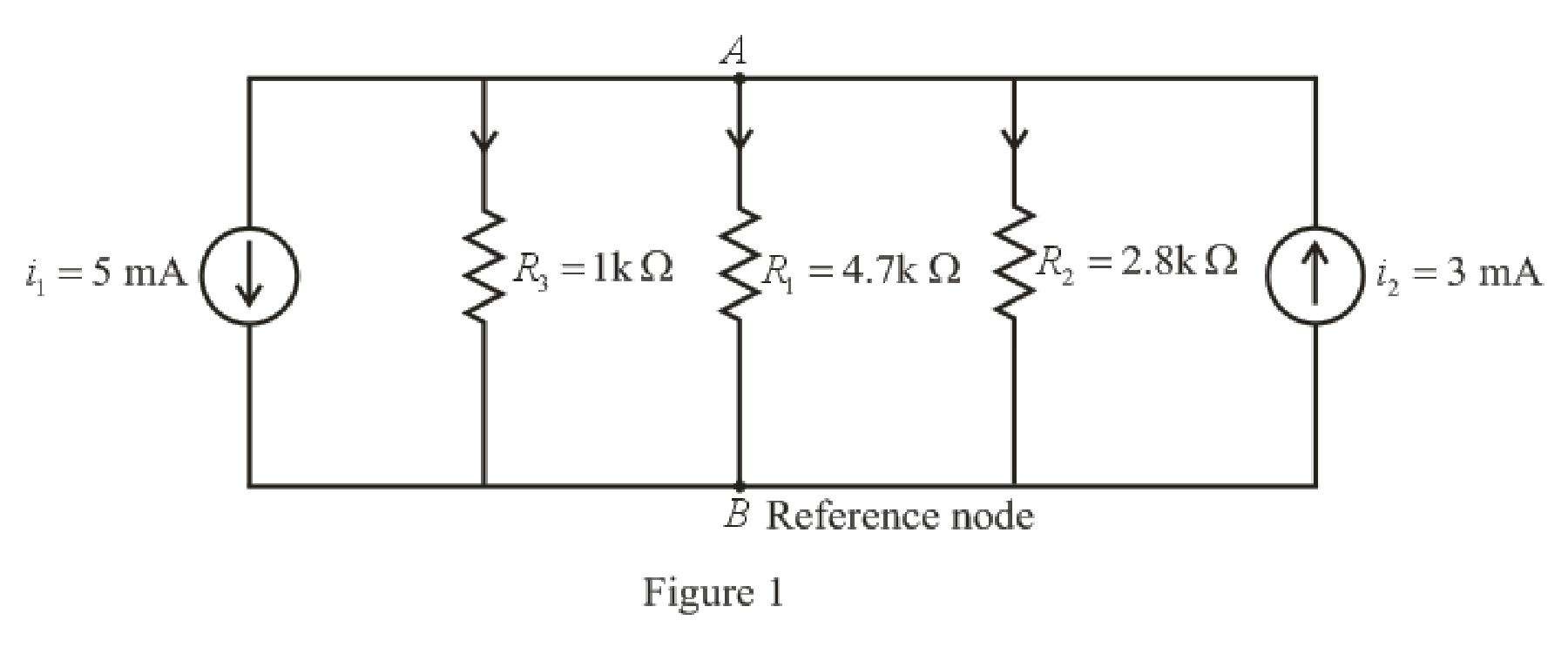
The circuit diagram is redrawn as shown in Figure 1.

Refer to the redrawn Figure 1.
The expression for KCL at node
Here,
The expression for power absorbed by resistor is as follows.
Here,
Refer to the redrawn Figure 1.
Substitute
Rearrange equation (3) for
Substitute
Simplify for
So, power absorbed by resistor
Substitute
Simplify for
So, the power absorbed by resistor
Substitute
So, the power absorbed by resistor
Conclusion:
Thus, the power absorbed by resistor
(b)
Find the power supplied by each current source.
Answer to Problem 34E
Power supplied by dependent current source
Explanation of Solution
Formula used:
The expression for power supplied by current source is as follows.
Here,
Calculation:
Refer to the redrawn Figure 1.
As current direction for independent current source
Substitute
So power supplied by dependent current source
Substitute
So power supplied by dependent current source
Conclusion:
Thus, the power supplied by dependent current source
(c)
Verify that sum of power absorbed and sum of power supplied in the circuit is same.
Answer to Problem 34E
Sum of power absorbed and sum of power supplied in the circuit is same.
Explanation of Solution
Formula used:
The expression for power is as follows.
Here,
Calculation:
Substitute
So, the total power absorbed is
Substitute
So total power supplied is
Conclusion:
Thus, sum of power absorbed and sum of power supplied in the circuit is same.
Want to see more full solutions like this?
Chapter 3 Solutions
ENGINEERING CIRCUIT...(LL)>CUSTOM PKG.<
- can you fin Vds and Vgs of all transistors and specify te operating region off all transistors and prove it. 58V 5.8 V 1.8V M2 0.9V 22222 と A 4852 m 3 01 A Voy = 0.2 V V4)=0.SV λ=0.1 V-1arrow_forwardNeed a aolarrow_forward2 Find Inverse Fourier transform of F(jw) = 2w -16+w2, and plot the f(t).arrow_forward
- 5.25. Determine the corner frequency resulting from Cin in Fig. 5.47(d). For simplicity, assume C₁ is a short circuit. TVDD C₁ M2 RF Vin H w - Vout Cin M₁arrow_forwardIn the below circuit, find out the value of equivalent Thevenin's voltage and Thevenin's resistance at the terminal. 2000 0.25 A 400 2 800 2 0.1 Aarrow_forwardQ1: For the circuit shown in Figure-1, (a) Calculate the equivalent resistance of the circuit, RAB at the terminals A and B. [10] (b) When 50V dc source is switched at terminals A-B, solve for the voltage V₁ at the location shown. [10] 50V www 12Ω 10Ω 5Ω www www A + B 200 Figure-1 www 10Ω ww 25Ω 100arrow_forward
 Introductory Circuit Analysis (13th Edition)Electrical EngineeringISBN:9780133923605Author:Robert L. BoylestadPublisher:PEARSON
 Delmar's Standard Textbook Of ElectricityElectrical EngineeringISBN:9781337900348Author:Stephen L. HermanPublisher:Cengage Learning
 Programmable Logic ControllersElectrical EngineeringISBN:9780073373843Author:Frank D. PetruzellaPublisher:McGraw-Hill Education
 Fundamentals of Electric CircuitsElectrical EngineeringISBN:9780078028229Author:Charles K Alexander, Matthew SadikuPublisher:McGraw-Hill Education
 Electric Circuits. (11th Edition)Electrical EngineeringISBN:9780134746968Author:James W. Nilsson, Susan RiedelPublisher:PEARSON
 Engineering ElectromagneticsElectrical EngineeringISBN:9780078028151Author:Hayt, William H. (william Hart), Jr, BUCK, John A.Publisher:Mcgraw-hill Education,


