Concept explainers
Videos
a.
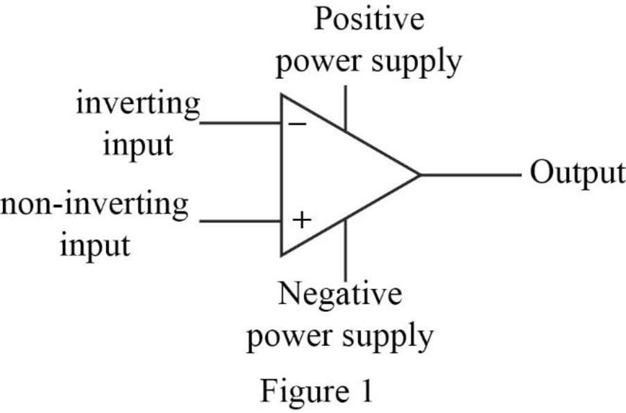
Label the five terminals in the operational amplifier.
a.
Explanation of Solution
Given data:
Refer to the given op amp circuit.
Discussion:
The five terminals of the op amp are labeled and it is shown in Figure 1.
Conclusion:
Thus, the five terminals in the operational amplifier are labeled.
b.
Mention the parameter that constraints the value of
b.
Answer to Problem 1P
The input resistance of the op amp constraints the value of
Explanation of Solution
Discussion:
The input resistance of an ideal op amp is infinite, which restricts the current
Conclusion:
Thus, the input resistance of the op amp constraints the value of
c.
Mention the parameter that constraints the value of
c.
Answer to Problem 1P
The open loop voltage gain of the op amp constraints the value of
Explanation of Solution
Discussion:
The open loop voltage gain of an ideal op amp is infinite, which constraints the difference between the voltage appear across the inverting and non-inverting terminal of the op amp to 0 V. Therefore,
Conclusion:
Thus, the open loop voltage gain of the op amp constraints the value of
d.
Find the value of voltage
d.
Answer to Problem 1P
The value of voltage
Explanation of Solution
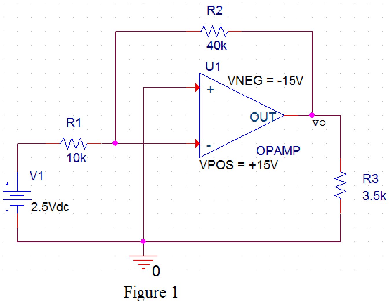
PSpice design:
Draw the given circuit in PSPICE as shown in Figure 2.
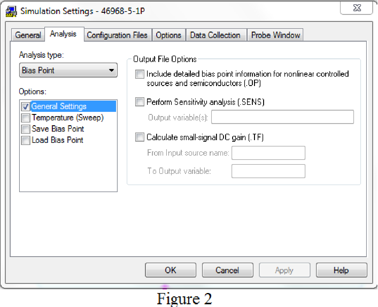
Provide the simulation settings as shown in Figure 3 to obtain output parameters.
After simulating the PSPICE circuit, the output voltage
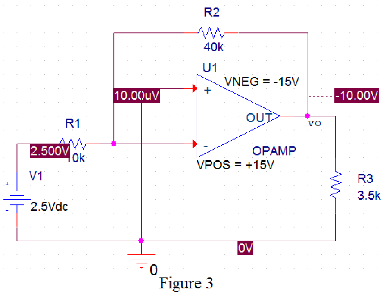
From Figure 4, the output voltage
Conclusion:
Thus, the value of voltage
Want to see more full solutions like this?
Chapter 5 Solutions
Electric Circuits. (11th Edition)
Additional Engineering Textbook Solutions
Concepts Of Programming Languages
Computer Science: An Overview (13th Edition) (What's New in Computer Science)
Electric Circuits. (11th Edition)
Starting Out with Python (4th Edition)
Modern Database Management
Java: An Introduction to Problem Solving and Programming (8th Edition)


- 9.34 Consider the finite-state machine logic implementation in Figure P9.34. (a) Determine the next-state and output logic expressions. (b) Determine the number of possible states. (c) Construct a state assigned table. (d) Construct a state table. (e) Construct a state diagram. (f) Determine the function of the finite-state machine. T₁ x Clk Figure P9.34 Q Clk Q الا T₂ Q 32 Clk Q T3 Q Clk Q Узarrow_forward9.35 Consider the finite-state machine logic implementation in Figure P9.35. (a) Determine the next-state and output logic expressions. (b) Determine the number of possible states. (c) Construct a state assigned table. (d) Construct a state table. (e) Construct a state diagram. (f) Determine the function of the finite-state machine. Clk J Clk K₁ 10 Ут J2 Clk K₂ 10 32 Figure P9.35arrow_forward9.56 Using JK flip-flops, design a synchronous counter that counts in the sequence 1, 3, 0, 2, 1, ... The counter counts only when its enable input x is equal to 1; otherwise, the counter is idle.arrow_forward
- 9.65 Using T flip-flops, design a synchronous counter that counts in the sequence 0, 2, 4, 6, 0, ... The counter counts only when its enable input x is equal to 1; otherwise, the counter is idle.arrow_forward2 Using D flip-flops, design a synchronous counter that counts in the sequence 1, 4, 7, 1, The counter counts only when its enable input x is equal to 1; otherwise, the counter is idle.arrow_forwardQ1: Write a VHDL code to implement the finite state machine described in the state diagram shown below. Clk D 0 CIK Q D 0 Cik Q =arrow_forward
- Q1: Consider the finite state machine logic implementation in Fig. shown below: Construct the state diagram. Repeat the circuit design using j-k flip flop. r" Clk Y D' Y, Clk Q D Clk 10 0 22 3'2arrow_forwardQ: Write a VHDL code to implement the finite state machine described in the state diagram shown below. T 2 Clk Q Clk T₂ 0 la Clk T3 Q Cik 0arrow_forwardDo you happen to know what is the complete circuit?arrow_forward
- b) Draw the magnitude and phase bode plot c) Given Cdb=0.02pF, how will the frequency response change, draw the resulting magnitude and phase bode plotplz help me to solve part b and c.arrow_forwardMedium 1 is a lossless dielectric (ε₁, μ₁ = μo, σ₁ = 0) Medium 2 is a perfect electric conductor (PEC) ( 2 = 0, μ2 = μo, σ₂ = ∞) [ Moσ = 0] [ε0 μ₁ σ₂ = ∞ ] (J=σE is finite, E = 0) E(z) Exe² +Пe₁²] 1. For the case εr] = λι = = E2(z)-0 - 1 (vacuum), E₁x 1 V/m and a frequency f = 500 MHz determine: n₁ = 12= 2. Determine: r = T= 3. Using this I show that the total electric field E₁0(z) in region 1 can be written as: E(z) = -2jE, sin(2лz/λ)✰ 4. The magnitude E10(z) will show an interference pattern. The SWR (standing wave ratio) is the Emax/Emin ratio of the magnitude of the total electric field in region 1. What is the SWR? E (z) = 2|E|sin(2лz/2₁)| E" (z) SWR A Imax E(z) Imin 1+r 1-|| tot 5. Roughly SKETCH the magnitude of E10(z) and E20(z) on the graph below. E₁tot(z) tot E20(z) -0.40 -0.30 -0.ło z=0 +0.1b +0.20arrow_forwardwould anyone be able to tell me the amount of wire needed for this electrical plan in this house? and if possible would anyone be able to tell me the amount of any other materials needed (wire sizes, box sizes/styles)arrow_forward
 Introductory Circuit Analysis (13th Edition)Electrical EngineeringISBN:9780133923605Author:Robert L. BoylestadPublisher:PEARSON
 Delmar's Standard Textbook Of ElectricityElectrical EngineeringISBN:9781337900348Author:Stephen L. HermanPublisher:Cengage Learning
 Programmable Logic ControllersElectrical EngineeringISBN:9780073373843Author:Frank D. PetruzellaPublisher:McGraw-Hill Education
 Fundamentals of Electric CircuitsElectrical EngineeringISBN:9780078028229Author:Charles K Alexander, Matthew SadikuPublisher:McGraw-Hill Education
 Electric Circuits. (11th Edition)Electrical EngineeringISBN:9780134746968Author:James W. Nilsson, Susan RiedelPublisher:PEARSON
 Engineering ElectromagneticsElectrical EngineeringISBN:9780078028151Author:Hayt, William H. (william Hart), Jr, BUCK, John A.Publisher:Mcgraw-hill Education,