Concept explainers
Videos
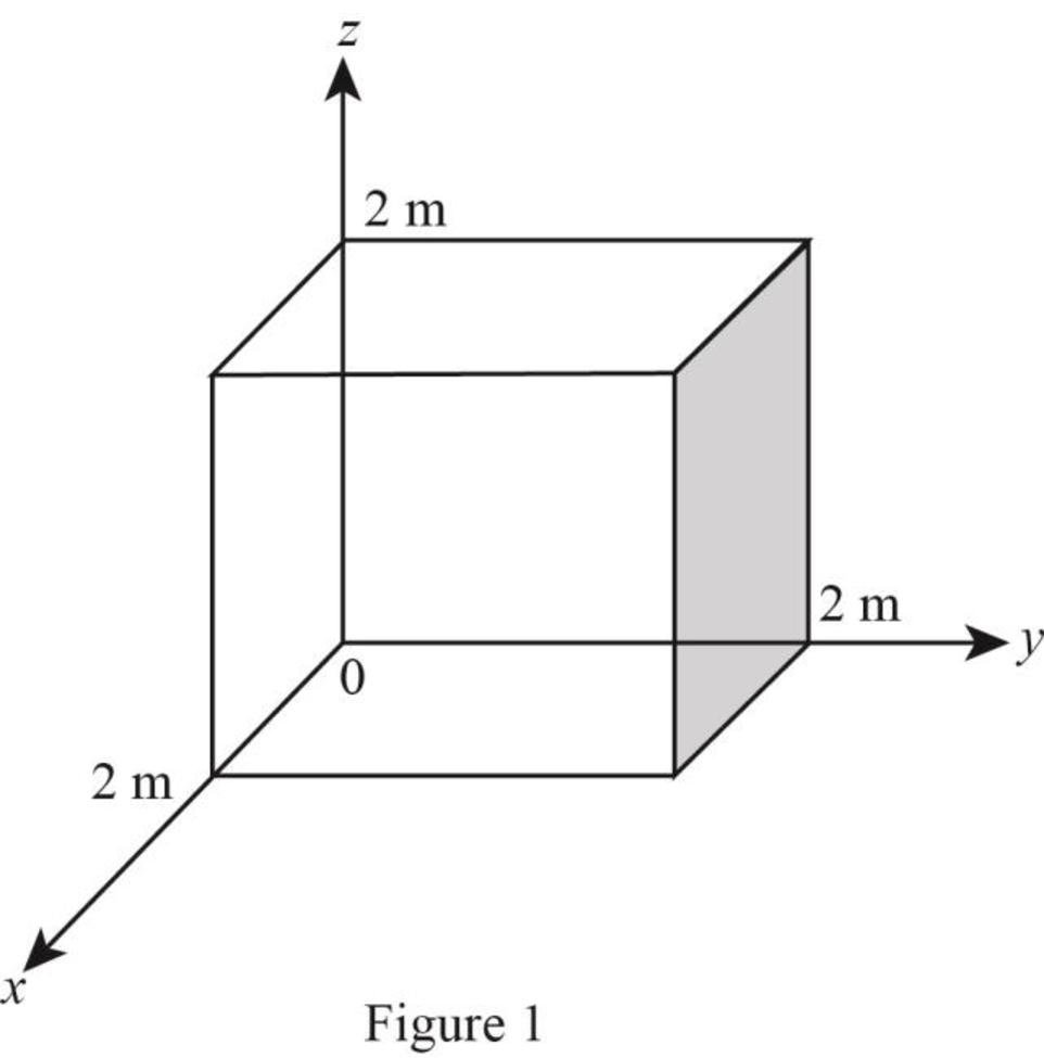
A cube 2 m on a side is located in the first octant in a Cartesian coordinate system, with one of its corners at the origin. Find the total charge contained in the cube if the charge density is given by ρv = xy2e−2z (mC/m3).
The total charge contained in the cube for the given conditions.
Answer to Problem 1P
The total charge contained in the cube for the given conditions is
Explanation of Solution
Given data:
The side of the cube is
The volume charge density is
Calculation:
The required diagram for the given condition is drawn as shown in Figure 1.
Write the standard expression of charge for volume charge density.
Here,
Differential volume in Cartesian coordinate system is,
The given cube is resting on one of its corner at origin and in the first quadrant.
Hence, range of
Range of
Range of
Substituting
Solve the above expression.
Conclusion:
Therefore, the total charge contained in the cube is
Want to see more full solutions like this?
Chapter 4 Solutions
Fundamentals of Applied Electromagnetics (7th Edition)


- Can you rewrite the solution because it is unclear? AM (+) = 8(1+ 0.5 cos 1000kt +0.5 ros 2000ks) = cos 10000 πt. 8 cos wat + 4 cos wit + 4 cos Wat coswet. -Jet jooort J11000 t = 4 e jqooort jgoort +4e + e +e j 12000rt. 12000 kt + e +e jooxt igoo t te (w) = 8ES(W- 100007) + 8IS (W-10000) USBarrow_forwardCan you rewrite the solution because it is unclear? AM (+) = 8(1+0.5 cos 1000kt +0.5 ros 2000 thts) = cos 10000 πt. 8 cos wat + 4 cos wit + 4 cos Wat coswet. J4000 t j11000rt $14+) = 45 jqooort +4e + e + e j 12000rt. 12000 kt + e +e +e Le jsoort -; goon t te +e Dcw> = 885(W- 100007) + 8 IS (W-10000) - USBarrow_forwardCan you rewrite the solution because it is unclear? Q2 AM ①(+) = 8 (1+0.5 cos 1000πt +0.5 ros 2000kt) $4+) = 45 = *cos 10000 πt. 8 cos wat + 4 cosat + 4 cos Wat coswet. j1000016 +4e -j10000πt j11000Rt j gooort -j 9000 πt + e +e j sooort te +e J11000 t + e te j 12000rt. -J12000 kt + с = 8th S(W- 100007) + 8 IS (W-10000) <&(w) = USB -5-5 -4-5-4 b) Pc 2² = 64 PSB = 42 + 4 2 Pt Pc+ PSB = y = Pe c) Puss = PLSB = = 32 4² = 8 w 32+ 8 = × 100% = 140 (1)³×2×2 31 = 20% x 2 = 3w 302 USB 4.5 5 5.6 6 ms Ac = 4 mi = 0.5 mz Ac = 4 ५ M2 = =0.5arrow_forward
- A. Draw the waveform for the following binary sequence using Bipolar RZ, Bipolar NRZ, and Manchester code. Data sequence= (00110100) B. In a binary PCM system, the output signal-to-quantization ratio is to be hold to a minimum of 50 dB. If the message is a single tone with fm-5 kHz. Determine: 1) The number of required levels, and the corresponding output signal-to-quantizing noise ratio. 2) Minimum required system bandwidth.arrow_forwardFind Io using Mesh analysisarrow_forwardFM station of 100 MHz carrier frequency modulated by a 20 kHz sinusoid with an amplitude of 10 volt, so that the peak frequency deviation is 25 kHz determine: 1) The BW of the FM signal. 2) The approximated BW if the modulating signal amplitude is increased to 50 volt. 3) The approximated BW if the modulating signal frequency is increased by 70%. 4) The amplitude of the modulating signal if the BW is 65 kHz.arrow_forward
- An FDM is used to multiplex two groups of signals using AM-SSB, the first group contains 25 speech signals, each has maximum frequency of 4 kHz, the second group contains 15 music signals, each has maximum frequency of 10 kHz. A guard bandwidth of 500 Hz is used bety each two signals and before the first one. 1. Find the BWmultiplexing 2. Find the BWtransmission if the multiplexing signal is modulated using AM-DSB-LC.arrow_forwardAn FM signal with 75 kHz deviation, has an input signal-to-noise ratio of 18 dB, with a modulating frequency of 15 kHz. 1) Find SNRO at demodulator o/p. 2) Find SNRO at demodulator o/p if AM is used with m=0.3. 3) Compare the performance in case 1) and 2).. Hint: for single tone AM-DSB-LC, SNR₁ = (2m²) (4)arrow_forwardFind Va and Vb using Nodal analysisarrow_forward
 Delmar's Standard Textbook Of ElectricityElectrical EngineeringISBN:9781337900348Author:Stephen L. HermanPublisher:Cengage Learning